MCP1825/MCP1825S
† Notice: Stresses above those listed under “Maximum Rat-
ings” may cause permanent damage to the device. This is a
stress rating only and functional operation of the device at
those or any other conditions above those indicated in the
operational listings of this specification is not implied. Expo-
sure to maximum rating conditions for extended periods may
affect device reliability.
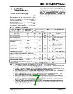
1.0
ELECTRICAL
CHARACTERISTICS
Absolute Maximum Ratings †
VIN....................................................................................6.5V
Maximum Voltage on Any Pin .. (GND – 0.3V) to (VDD + 0.3)V
Maximum Power Dissipation......... Internally-Limited (Note 6)
Output Short Circuit Duration................................Continuous
Storage temperature .....................................-65°C to +150°C
Maximum Junction Temperature, TJ ...........................+150°C
ESD protection on all pins (HBM/MM) ........... ≥ 4 kV; ≥ 300V
AC/DC CHARACTERISTICS
Electrical Specifications: Unless otherwise noted, VIN = VOUT(MAX) + VDROPOUT(MAX), Note 1, VR = 1.8V for Adjustable Output,
OUT = 1 mA, CIN = COUT = 4.7 µF (X7R Ceramic), TA = +25°C.
Boldface type applies for junction temperatures, TJ (Note 7) of -40°C to +125°C
I
Parameters
Sym
Min
Typ
Max
Units
Conditions
Input Operating Voltage
Input Quiescent Current
VIN
Iq
2.1
6.0
V
Note 1
—
120
0.1
220
µA
IL = 0 mA, VOUT = 0.8V to
5.0V
Input Quiescent Current for
SHDN Mode
ISHDN
IOUT
—
500
—
3
—
µA
mA
%/V
%
SHDN = GND
Maximum Output Current
—
VIN = 2.1V to 6.0V
V
R = 0.8V to 5.0V, Note 1
Line Regulation
ΔVOUT
(VOUT x ΔVIN
/
±0.05
±0.5
1.2
±0.16
1.0
—
(Note 1) ≤ VIN ≤ 6V
)
Load Regulation
ΔVOUT/VOUT
-1.0
—
IOUT = 1 mA to 500 mA,
(Note 4)
Output Short Circuit Current
IOUT_SC
A
RLOAD < 0.1Ω, Peak Current
Adjust Pin Characteristics (Adjustable Output Only)
Adjust Pin Reference Voltage
VADJ
0.402
0.410
0.418
V
VIN = 2.1V to VIN = 6.0V,
I
OUT = 1 mA
Adjust Pin Leakage Current
IADJ
-10
—
±0.01
40
+10
—
nA
VIN = 6.0V, VADJ = 0V to 6V
Adjust Temperature Coefficient
TCVOUT
ppm/°C Note 3
Fixed-Output Characteristics (Fixed Output Only)
Voltage Regulation VOUT
VR - 2.5% VR ±0.5% VR + 2.5%
V
Note 2
Note 1: The minimum VIN must meet two conditions: VIN ≥ 2.1V and VIN ≥ VOUT(MAX) + VDROPOUT(MAX).
2: VR is the nominal regulator output voltage for the fixed cases. VR = 1.2V, 1.8V, etc. VR is the desired set point output
voltage for the adjustable cases. VR = VADJ * ((R1/R2)+1). Figure 4-1.
3: TCVOUT = (VOUT-HIGH – VOUT-LOW) *106 / (VR * ΔTemperature). VOUT-HIGH is the highest voltage measured over the
temperature range. VOUT-LOW is the lowest voltage measured over the temperature range.
4: Load regulation is measured at a constant junction temperature using low duty-cycle pulse testing. Load regulation is
tested over a load range from 1 mA to the maximum specified output current.
5: Dropout voltage is defined as the input-to-output voltage differential at which the output voltage drops 2% below its
nominal value that was measured with an input voltage of VIN = VOUT(MAX) + VDROPOUT(MAX)
.
6: The maximum allowable power dissipation is a function of ambient temperature, the maximum allowable junction
temperature and the thermal resistance from junction to air. (i.e., TA, TJ, θJA). Exceeding the maximum allowable power
dissipation will cause the device operating junction temperature to exceed the maximum +150°C rating. Sustained
junction temperatures above 150°C can impact device reliability.
7: The junction temperature is approximated by soaking the device under test at an ambient temperature equal to the
desired junction temperature. The test time is small enough such that the rise in the junction temperature over the
ambient temperature is not significant.
© 2008 Microchip Technology Inc.
DS22056B-page 7

 MICROCHIP [ MICROCHIP ]