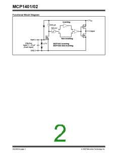
MCP1401/02
† Notice: Stresses above those listed under "Maximum
Ratings" may cause permanent damage to the device. This is
a stress rating only and functional operation of the device at
those or any other conditions above those indicated in the
operational sections of this specification is not intended.
Exposure to maximum rating conditions for extended periods
may affect device reliability.
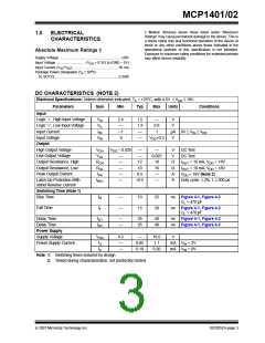
1.0
ELECTRICAL
CHARACTERISTICS
Absolute Maximum Ratings †
Supply Voltage ................................................................+20V
Input Voltage ...............................(VDD + 0.3V) to (GND – 5V)
Input Current (VIN>VDD)................................................50 mA
Package Power Dissipation (TA = 50oC)
5L SOT23..................................................................0.39W
DC CHARACTERISTICS (NOTE 2)
Electrical Specifications: Unless otherwise indicated, TA = +25°C, with 4.5V ≤ VDD ≤ 18V.
Parameters
Sym
Min
Typ
Max
Units
Conditions
Input
Logic ‘1’, High Input Voltage
Logic ‘0’, Low Input Voltage
Input Current
VIH
VIL
IIN
2.4
—
–1
-5
1.5
1.3
—
—
0.8
V
V
1
µA 0V ≤ VIN ≤ VDD
Input Voltage
VIN
—
VDD+0.3
V
Output
High Output Voltage
Low Output Voltage
Output Resistance, High
Output Resistance, Low
Peak Output Current
VOH
VOL
ROH
ROL
IPK
VDD – 0.025
—
—
—
0.025
18
V
V
Ω
Ω
A
A
DC Test
—
—
—
—
—
DC Test
12
IOUT = 10 mA, VDD = 18V
IOUT = 10 mA, VDD = 18V
VDD = 18V (Note 2)
Duty cycle ≤ 2%, t ≤ 300 µs
10
16
0.5
>0.5
—
Latch-Up Protection With-
stand Reverse Current
IREV
—
Switching Time (Note 1)
Rise Time
tR
tF
—
—
19
15
25
20
ns
ns
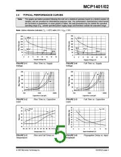
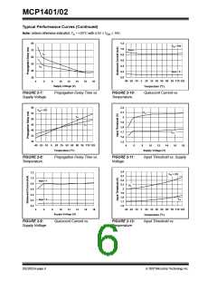
Figure 4-1, Figure 4-2
CL = 470 pF
Fall Time
Figure 4-1, Figure 4-2
CL = 470 pF
Delay Time
tD1
tD2
—
—
35
35
40
40
ns
ns
Figure 4-1, Figure 4-2
Figure 4-1, Figure 4-2
Delay Time
Power Supply
Supply Voltage
Power Supply Current
VDD
IS
4.5
—
—
18.0
1.1
V
0.85
0.10
mA VIN = 3V
mA VIN = 0V
IS
—
0.20
Note 1: Switching times ensured by design.
2: Tested during characterization, not production tested.
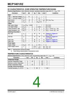
© 2007 Microchip Technology Inc.
DS22052A-page 3

 MICROCHIP [ MICROCHIP ]