HCS301
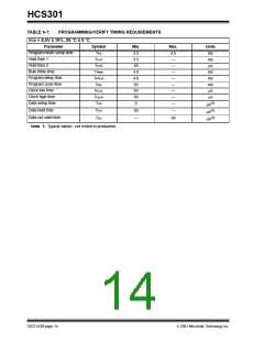
programming delay is required for the internal program
cycle to complete. This delay can take up to TWC. At the
end of the programming cycle, the device can be veri-
fied (Figure 6-2) by reading back the EEPROM. Read-
ing is done by clocking the S2 (or S3) line and reading
the data bits on PWM. For security reasons, it is not
possible to execute a verify function without first pro-
gramming the EEPROM. A Verify operation can only
be done once, immediately following the Program
cycle.
6.0
PROGRAMMING THE HCS301
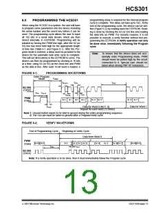
When using the HCS301 in a system, the user will have
to program some parameters into the device including
the serial number and the secret key before it can be
used. The programming cycle allows the user to input
all 192 bits in a serial data stream, which are then
stored internally in EEPROM. Programming will be
initiated by forcing the PWM line high, after the S2 (or
S3) line has been held high for the appropriate length
of time line (Table 6-1 and Figure 6-1). After the Pro-
gram mode is entered, a delay must be provided to the
device for the automatic bulk write cycle to complete.
This will set all locations in the EEPROM to zeros. The
device can then be programmed by clocking in 16 bits
at a time, using S2 (or S3) as the clock line and PWM
as the data in line. After each 16-bit word is loaded, a
Note: To ensure that the device does not acci-
dentally enter Programming mode, PWM
should never be pulled high by the circuit
connected to it. Special care should be
taken when driving PNP RF transistors.
FIGURE 6-1:
PROGRAMMING WAVEFORMS
Enter Program
Mode
TPBW
TDS
TCLKH
TWC
S2 (S3)
(Clock)
TPS
TPH1
TDH
Bit 3
TCLKL
Bit 0 Bit 1
PWM
(Data)
Bit 2
Bit 14 Bit 15
Bit 16 Bit 17
Data for Word 1
Data for Word 0 (KEY_0)
Repeat for each word (12 times)
TPH2
Note 1: Unused button inputs to be held to ground during the entire programming sequence.
2: The VDD pin must be taken to ground after a Program/Verify cycle.
FIGURE 6-2:
VERIFY WAVEFORMS
Beginning of Verify Cycle
Data from Word 0
End of Programming Cycle
PWM
(Data)
Bit190 Bit191
Bit 0
Bit 1 Bit 2 Bit 3
Bit 14
Bit 15
Bit 16 Bit 17
Bit190 Bit191
TWC
TDV
S2 (S3)
(Clock)
Note: If a Verify operation is to be done, then it must immediately follow the Program cycle.
2001 Microchip Technology Inc.
DS21143B-page 13

 MICROCHIP [ MICROCHIP ]