ATmega48/88/168
15.1.1
Registers
The Timer/Counter (TCNT2) and Output Compare Register (OCR2A and OCR2B) are 8-bit reg-
isters. Interrupt request (shorten as Int.Req.) signals are all visible in the Timer Interrupt Flag
Register (TIFR2). All interrupts are individually masked with the Timer Interrupt Mask Register
(TIMSK2). TIFR2 and TIMSK2 are not shown in the figure.
The Timer/Counter can be clocked internally, via the prescaler, or asynchronously clocked from
the TOSC1/2 pins, as detailed later in this section. The asynchronous operation is controlled by
the Asynchronous Status Register (ASSR). The Clock Select logic block controls which clock
source he Timer/Counter uses to increment (or decrement) its value. The Timer/Counter is inac-
tive when no clock source is selected. The output from the Clock Select logic is referred to as the
timer clock (clkT2).
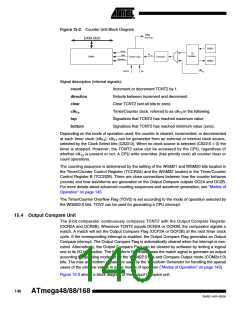
The double buffered Output Compare Register (OCR2A and OCR2B) are compared with the
Timer/Counter value at all times. The result of the compare can be used by the Waveform Gen-
erator to generate a PWM or variable frequency output on the Output Compare pins (OC2A and
OC2B). See Section “15.4” on page 140. for details. The compare match event will also set the
Compare Flag (OCF2A or OCF2B) which can be used to generate an Output Compare interrupt
request.
15.1.2
Definitions
Many register and bit references in this document are written in general form. A lower case “n”
replaces the Timer/Counter number, in this case 2. However, when using the register or bit
defines in a program, the precise form must be used, i.e., TCNT2 for accessing Timer/Counter2
counter value and so on.
The definitions in Table 15-1 are also used extensively throughout the section.
Table 15-1. Definitions
BOTTOM
MAX
The counter reaches the BOTTOM when it becomes zero (0x00).
The counter reaches its MAXimum when it becomes 0xFF (decimal 255).
TOP
The counter reaches the TOP when it becomes equal to the highest value in the
count sequence. The TOP value can be assigned to be the fixed value 0xFF
(MAX) or the value stored in the OCR2A Register. The assignment is depen-
dent on the mode of operation.
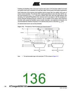
15.2 Timer/Counter Clock Sources
The Timer/Counter can be clocked by an internal synchronous or an external asynchronous
clock source. The clock source clkT2 is by default equal to the MCU clock, clkI/O. When the AS2
bit in the ASSR Register is written to logic one, the clock source is taken from the Timer/Counter
Oscillator connected to TOSC1 and TOSC2. For details on asynchronous operation, see ”Asyn-
chronous Status Register – ASSR” on page 156. For details on clock sources and prescaler, see
”Timer/Counter Prescaler” on page 158.
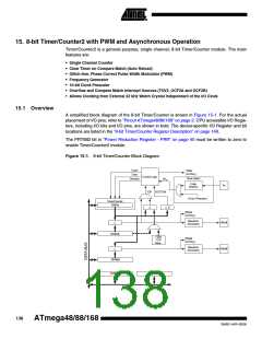
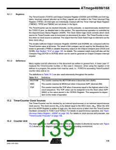
15.3 Counter Unit
The main part of the 8-bit Timer/Counter is the programmable bi-directional counter unit. Figure
15-2 shows a block diagram of the counter and its surrounding environment.
139
2545E–AVR–02/05

 MICROCHIP [ MICROCHIP ]