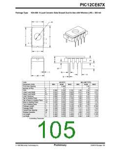
PIC12CE67X
PS2 bit ................................................................................ 16
PSA bit................................................................................ 16
PUSH.................................................................................. 22
Timers
Timer0
Block Diagram.................................................... 31
External Clock .................................................... 33
External Clock Timing ........................................ 33
Increment Delay ................................................. 33
Interrupt.............................................................. 31
Interrupt Timing .................................................. 32
Prescaler ............................................................ 34
Prescaler Block Diagram.................................... 34
Section ............................................................... 31
Switching Prescaler Assignment........................ 35
Synchronization.................................................. 33
T0CKI ................................................................. 33
T0IF.................................................................... 56
Timing................................................................. 31
TMR0 Interrupt ................................................... 56
R
RC Oscillator....................................................................... 47
Read Modify Write .............................................................. 26
Read-Modify-Write.............................................................. 26
Register File........................................................................ 11
Registers
Map
PIC12CE67X ...................................................... 12
Reset Conditions......................................................... 51
Reset............................................................................. 45, 48
Reset Conditions for Special Registers .............................. 51
RETFIE Instruction.............................................................. 70
RETLW Instruction.............................................................. 70
RETURN Instruction ........................................................... 71
RLF Instruction.................................................................... 71
RP0 bit .......................................................................... 11, 15
RP1 bit ................................................................................ 15
RRF Instruction................................................................... 71
Timing Diagrams
A/D Conversion .......................................................... 97
CLKOUT and I/O ........................................................ 92
External Clock Timing................................................. 90
Time-out Sequence .................................................... 52
Timer0 .................................................................. 31, 94
Timer0 Interrupt Timing .............................................. 32
Timer0 with External Clock......................................... 33
Wake-up from Sleep via Interrupt............................... 59
TO bit.................................................................................. 15
TOSE bit............................................................................. 16
TRIS Instruction.................................................................. 73
TRIS Register......................................................... 14, 25, 26
Two’s Complement................................................................7
S
SEEVAL Evaluation and Programming System............... 77
Services
One-Time-Programmable (OTP) .................................. 5
Quick-Turnaround-Production (QTP)............................ 5
Serialized Quick-Turnaround Production (SQTP)......... 5
SFR..................................................................................... 62
SFR As Source/Destination ................................................ 62
SLEEP .......................................................................... 45, 48
SLEEP Instruction............................................................... 71
Software Simulator (MPLAB-SIM) ...................................... 77
Special Features of the CPU .............................................. 45
Special Function Register
U
UV Erasable Devices.............................................................5
W
PIC12CE67X............................................................... 13
Special Function Registers ................................................. 62
Special Function Registers, Section ................................... 12
Stack................................................................................... 22
Overflows.................................................................... 22
Underflow.................................................................... 22
STATUS Register ............................................................... 15
SUBLW Instruction.............................................................. 72
SUBWF Instruction ............................................................. 72
SWAPF Instruction.............................................................. 73
W Register
ALU................................................................................7
Wake-up from SLEEP ........................................................ 58
Watchdog Timer (WDT).................................... 45, 48, 51, 57
WDT ................................................................................... 51
Block Diagram ............................................................ 57
Period ......................................................................... 57
Programming Considerations..................................... 57
Timeout....................................................................... 51
WWW, On-Line Support........................................................2
T
X
T0CS bit.............................................................................. 16
TAD...................................................................................... 41
Timer0
XORLW Instruction............................................................. 73
XORWF Instruction............................................................. 73
Z
RTCC.......................................................................... 51
Z bit..................................................................................... 15
Zero bit ..................................................................................7
1998 Microchip Technology Inc.
Preliminary
DS40181B-page 109

 MICROCHIP [ MICROCHIP ]