ML65244/ML65L244
line drivers, but it is not true for the ML65244 and
ML65L244. This is because their sink and source current
capability depends on the voltage difference between the
output and the input. The ML65244 can sink or source
more than 100mA to a load when the load is switching
due to the fact that during the transition, the difference
FUNCTIONAL DESCRIPTION
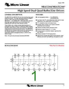
The ML65244 and ML65L244 are very high speed non-
inverting buffer/line drivers with three-state outputs which
are ideally suited for bus-oriented applications. They
provide a low propagation delay by using an analog
design approach (a high speed unity gain buffer), as
compared to conventional digital approaches. The
ML65244 and ML65L244 follow the pinout and
between the input and output is large. I is only
OL
significant as a DC specification, and is 25mA.
functionality of the industry standard FCT244 series of
buffer/line drivers and are intended to replace them in
designs where the propagation delay is a critical part of
the system design considerations. The ML65244 and
ML65L244 are capable of driving load capacitances
several times larger than their input capacitance. They are
configured so that the Ai inputs go to the YAi outputs, with
the A side output enable controlled by 1G. Similarly, 2G
controls the Bi inputs which go to the YBi outputs.
ARCHITECTURAL DESCRIPTION
Until now, buffer/line drivers have been implemented in
CMOS logic and made to be TTL compatible by sizing the
input devices appropriately. In order to buffer large
capacitances with CMOS logic, it is necessary to cascade
an even number of inverters, each successive inverter
larger than the preceding, eventually leading to an inverter
that will drive the required load capacitance at the
required frequency. Each inverter stage represents an
additional delay in the gating process because in order for
a single gate to switch, the input must slew more than half
of the supply voltage. The best of these CMOS buffers has
managed to drive a 50pF load capacitance with a delay of
3.2ns. Micro Linear has produced a dual quad buffer/line
driver with a delay less than 1.7ns by using a unique
circuit architecture that does not require cascaded logic
gates. The ML65244 uses a feedback technique to
produce an output that follows the input. If the output
voltage is not close to the input, then the feedback
circuitry will source or sink enough current to the load
capacitance to correct the discrepancy.
These unity gain analog buffers achieve low propagation
delays by having the output follow the input with a small
offset. The output rise and fall times will closely match
those of the input waveform. All inputs and outputs have
Schottky clamp diodes to handle undershoot or overshoot
noise suppression in unterminated applications. All
outputs have ground bounce suppression (typically
< 400mV), high drive output capability with almost
immediate response to the input signal, and low
output skew.
The I current drive capability of a buffer/line driver is
OL
often interpreted as a measure of its ability to sink current
in a dynamic sense. This may be true for CMOS buffer/
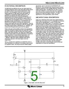
VCC
R8
Q1
Q2
R7
R3
R4
R2
R1
IN
OUT
Q4
Q6
Q5
Q7
Q3
R5
R6
GND
Figure 5. One buffer cell of the ML65244
5

 MICRO-LINEAR [ MICRO LINEAR CORPORATION ]