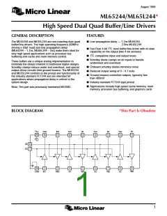
ML65244/ML65L244
ELECTRICAL CHARACTERISTICS
Unless otherwise stated, these specifications apply for: V = 5.0 ± 5%V, T = 0°C to 70°C (Note 1).
CC
A
SYMBOL
PARAMETER
CONDITIONS
MIN
TYP
MAX
UNITS
AC ELECTRICAL CHARACTERISTICS (CLOAD = 50pF, RLOAD = 500Ω)
tPLH, tPHL Propagation delay Ai to YAi, Bi to YBi (Note 2)
ML65244
1.4
1.6
10
1.7
2.0
15
ns
ns
ns
ML65L244
tOE
tOD
CIN
Output enable time
1G, 2G to YAi/YBi
Output disable time
1G, 2G to YAi/YBi
10
ns
Input capacitance
8
pF
DC ELECTRICAL CHARACTERISTICS (CLOAD = 50pF, RLOAD = ∞)
VIH
VIL
IIH
Input high voltage
Input low voltage
Input high current
Logic HIGH
2.0
V
Logic LOW
0.8
1.5
0.5
3.5
1.0
5
V
Per pin, VIN = 3V
ML65244
ML65L244
ML65244
ML65L244
0.5
0.3
2.4
0.8
mA
mA
mA
mA
µA
mA
IIL
Input low current
Per pin, VIN = 0
IHI-Z
IOS
Three-state output current VCC = 5.25V, 0 < VIN < VCC
Short circuit current
VCC = 5.25V, VO = GND
(Note 3)
–60
2.4
–225
VIC
Input clamp voltage
Output high voltage
VCC = 4.75V, IIN = 18mA
–0.7
–1.2
0.6
V
V
VOH
VCC = 4.75V, IOH = 100µA
(Notes 4 & 5)
VOL
Output low voltage
VCC = 4.75V, IOL = 25mA
(Notes 4 & 5)
V
VOFF
VIN – VOUT per buffer
VCC = 4.75V (Note 4)
ML65244
0
0
100
200
55
200
300
80
mV
mV
mA
ML65L244
ICC
Quiescent Power
Supply Current
VCC = 5.25V, Freq = 0Hz,
Inputs/outputs open
Note 1: Limits are guaranteed by 100% testing, sampling or correlation with worst case test conditions.
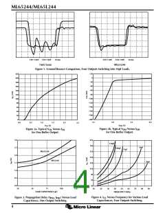
Note 2: One line switching, see Figure 3, tPLH, tPHL versus CL.
Note 3: Not more than one output should be shorted for more than a second.
Note 4: This is a true analog buffer. In the linear region, the output tracks the input with an offset (VOFF). For VOH, VIN = 2.7V.
VOH MIN includes VOFF. For VOL, VIN = 0V, VOL MAX includes VOFF
Note 5: See Figure 2 for IOH versus VOH and IOL versus VOL data.
t , t ≤ 4ns
R
F
3V
INPUT
1.5V
1.5V
0V
3V
t
t
PLH
PHL
OUTPUT
1.5V
1.5V
0V
3

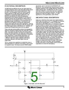
 MICRO-LINEAR [ MICRO LINEAR CORPORATION ]