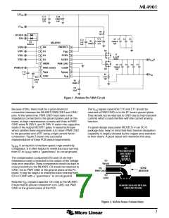
ML4901
12VIN
5VIN
C10
220nF
16V
C11
22µF
25V
R4
1kΩ
OUTEN
UP#
C12
220nF
16V
3X
C1
C2
C3
C13
1µF
16V
R5
100kΩ
1800µF
10V
D1
BAW56
ML4901
1
2
3
4
5
6
7
8
16
15
14
13
12
11
10
9
D0
PROTECT
VID0
VID1
VID2
VID3
Q1
Q2
D1
V
DD
L2
2.5.µH
D2
P DRV
N DRV
D3
VCC
P
SHDN
PWR GOOD
PWR GND
COMP
4X C4
1800µF
10V
C5
C6
C7
PWRGD
C14
1nF
V
REF
GND
I
SENSE
R1
6mΩ
1W
VSS
V
FB
C8
220nF
16V
R3
330kΩ
C9
33pF
Figure 1. Pentium ProVRM Circuit
Because of this, there must be a good electrical
The V bypass capacitors C10 and C11 should be
DD
connection between the ML4901 PWR GND and GND
pins. At the same time, PWR GND must have a low
impedance connection to the ground plane used on the
board, as high instantaneous currents will flow in PWR
GND when N DRV L and N DRV H switch the capacitive
loads of the output MOSFET gates. A layout technique
which satisfies these requirements is to return PWR GND
to the grounded end of R1 using a high current Kelvin
connection. Figure 2 shows one successful
returned to PWR GND or to the PC board ground plane.
They should not be returned to GND due to high transient
currents which could interfere with the current sensing
function.
If a given design uses power MOSFETs in an SO-8
package style, keep in mind that their thermal dissipation
capability is largely dictated by the copper area available
to their drains. A good layout will maximize this area.
implementation of these PCB layout requirements.
I
is an input to a medium-speed, high-sensitivity
SENSE
TO
comparator. It is often helpful to shield the trace running
from R1 to I with a “guard trace” to circuit ground.
SYNCHRONOUS
RECTIFIER
SENSE
MOSFET
SOURCE
The compensation components R3 and C9 are high-
impedance nodes connected to the output of the voltage
loop error amplifier. These components should be kept in
close proximity to the ML4901. C9 should be returned to
GND, not to PWR GND or the ground plane of the PC
board. It may be helpful to shield the trace running from
R3 to COMP with a “guard trace” to circuit ground.
TO
SENSE
I
SENSE
RESISTOR
TO
PWR GND
TO
GND
Keep the V bypass capacitor C8 close to the ML4901.
REF
Ensure that its ground connection is to GND, not PWR
GND or the ground plane of the PCB.
POWER GROUND RETURN
(GROUND PLANE)
Figure 2. Kelvin Sense Connections
7

 MICRO-LINEAR [ MICRO LINEAR CORPORATION ]