Micrel
MIC4830
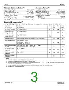
Absolute Maximum Ratings(1)
Operating Ratings(2)
Supply Voltage (VDD)...................................... –0.5V to 6.0V
Output Voltage (VCS) ..................................... –0.5V to 120V
EL Lamp Terminals (VA, VB)................................. VCS + 3V
Switch Voltage (Vsw)…………………………..-0.5V to 120V
Frequency Control Voltage
Supply Voltage (VDD).................................... +1.8V to +5.5V
Lamp Drive Frequency (fEL) ....................... 60Hz to 1000Hz
Switching Frequency (fSW).........................65kHz to 250kHz
Ambient Temperature (TA) ..........................–40°C to +85°C
Package Thermal Resistance(3)
(VRSW, VREL)................................... –0.5V to (VDD+0.3V)
MSOP (θJA) ......................................................206°C/W
MLF®-8L (θJA).....................................................63°C/W
Storage Temperature (TS).........................–65°C to +150°C
ESD Rating(4)...............................................................1.5kV
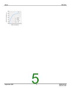
Electrical Characteristics(5)
VIN = VDD = 3.0V, RSW = 332KΩ, REL = 1.78MΩ. TA = 25°C unless otherwise specified. Bold values indicate –40°C ≤ TA ≤ +85°C.
Parameter
Condition
Min
Typ
3.8
88
Max
7
Units
Ohm
V
On-resistance
CS Voltage Variation
ISW = 100mA
VDD = 1.8V to 5.5V
VDD = 1.8V to 5.5V
76
99
Enable Input Low
Voltage (turn-off)
0.5
V
Enable Input High
Voltage (turn-on)
VDD = 1.8V to 5.5V
VDD-
0.5
V
Shutdown current
R
R
R
SW Resistor = LOW; REL Resistor = LOW; VDD = 5.5V
SW Resistor = HIGH;
0.01
0.5
75
µA
Input supply current
µA
EL Resistor = HIGH;
45
15
VCS = 90V; V
A
, V OPEN
B
Input current including
inductor
V
IN = VDD = 3.2V; Rsw = 290KΩ; Rel = 1.78MΩ;
mA
Hz
kHz
%
L=220µH; Rout=10kΩ; Lamp = 2in2
REL=1.78MΩ
VA
–V output drive
B
158
90
200
112
90
242
134
frequency
Switching transistor
frequency
RSW=332KΩ
Switching transistor
duty cycle
Notes:
1. Exceeding the absolute maximum rating may damage the device.
2. The device is not guaranteed to function outside its operating rating.
3. The maximum allowable power dissipation of any TA (ambient temperature) is PD(max) = (TJ(max) – TA) / θJA. Exceeding the maximum allowable
power dissipation will result in excessive die temperature.
4. Devices are ESD sensitive. Handling precautions recommended. Human body model, 1.5k in series with 100pF.
5. Specification for packaged product only.
M9999-091307
(408) 955-1690
September 2007
3

 MICREL [ MICREL SEMICONDUCTOR ]