MIC39500/39501
Micrel
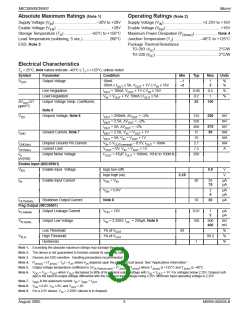
Absolute Maximum Ratings (Note 1)
Operating Ratings (Note 2)
Supply Voltage (V )
–20V to +20V
Supply Voltage (V )
+2.25V to +16V
+16V
IN
IN
Enable Voltage (V
)
+20V
–65°C to +150°C
260°C
Enable Voltage (V
)
EN
EN
Storage Temperature (T )
Maximum Power Dissipation (P
)
D(max)
Note 4
S
Lead Temperature (soldering, 5 sec.)
Junction Temperature (T )
–40°C to +125°C
J
ESD, Note 3
Package Thermal Resistance
TO-263 (θ
)
2°C/W
2°C/W
JC
JC
TO-220 (θ
)
Electrical Characteristics
TJ = 25°C, bold values indicate –40°C ≤ TJ ≤ +125°C; unless noted
Symbol
Parameter
Condition
Min
Typ
Max
Units
VOUT
Output Voltage
10mA
–1
–2
1
2
%
%
10mA ≤ IOUT ≤ 5A, VOUT + 1V ≤ VIN ≤ 16V
IOUT = 10mA, VOUT + 1V ≤ VIN ≤ 16V
VIN = VOUT + 1V, 10mA ≤ IOUT ≤ 5A
Line Regulation
0.06
0.2
20
0.5
1
%
%
Load Regulation
∆VOUT/∆T
ppm/°C
Output Voltage Temp. Coefficient,
100
Note 5
VDO
Dropout Voltage, Note 6
IOUT = 250mA, ∆VOUT = –2%
IOUT = 2.5A, ∆VOUT = –2%
125
320
400
15
250
mV
mV
mV
mA
mA
mA
A
IOUT = 5A, ∆VOUT = –2%
575
50
IGND
Ground Current, Note 7
IOUT = 2.5A, VIN = VOUT + 1V
IOUT = 5A, VIN = VOUT + 1V
70
IGND(do)
IOUT(lim)
Dropout Ground Pin Current
Current Limit
VIN ≤ VOUT(nominal) – 0.5V, IOUT = 10mA
VOUT = 0V, VIN = VOUT + 1V
2.1
7.5
260
en
Output Noise Voltage
COUT = 47µF, IOUT = 100mA, 10Hz to 100kHz
µV(rms)
Enable Input (MIC39501)
VEN Enable Input Voltage
logic low (off)
logic high (on)
VEN = VIN
0.8
V
V
2.25
IIN
Enable Input Current
30
10
35
75
µA
µA
VEN = 0.8V
2
4
µA
µA
IOUT(shdn)
Shutdown Output Current
Note 8
20
µA
Flag Output (MIC39501)
IFLG(leak) Output Leakage Current
VOH = 16V
0.01
180
1
2
µA
µA
VFLG(do)
Output Low Voltage
VIN = 2.250V, IOL, = 250µA, Note 9
300
400
mV
mV
Low Threshold
High Threshold
Hysteresis
1% of VOUT
1% of VOUT
93
%
%
%
VFLG
99.2
1
Note 1. Exceeding the absolute maximum ratings may damage the device.
Note 2. The device is not guaranteed to function outside its operating rating.
Note 3. Devices are ESD sensitive. Handling precautions recommended.
Note 4. PD(max) = (TJ(max) – TA) θJA, where θJA
depends upon the printed circuit layout. See “Applications Information.”
Note 5. Output voltage temperature coefficient is ∆VOUT(worst case) (TJ(max) – TJ(min)) where TJ(max) is +125°C and TJ(min) is –40°C.
Note 6. VDO = VIN – VOUT when VOUT decreases to 98% of its nominal output voltage with VIN = VOUT + 1V. For voltages below 2.25V, Dropout volt-
age is the input-to-output voltage differential with the minimum input voltage being 2.25V. Minimum input operating voltage is 2.25V.
Note 7. IGND is the quiescent current. IIN = IGND + IOUT
Note 8. VEN ≤ 0.8V, VIN ≤ 8V, and VOUT = 0V
Note 9. For a 2.5V device, VIN = 2.250V (device is in dropout).
August 2005
3
M9999-082605-B

 MICREL [ MICREL SEMICONDUCTOR ]