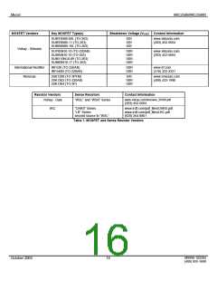
Micrel
MIC2586/MIC2586R
removed/cycled, or c) the ON pin is toggled LOW then HIGH.
The duty cycle of the auto-restart function is therefore fixed
at 5% and the period of the auto-restart cycle is given by:
Power-is-Good output signals PWRGD2 (/PWRGD2) and
PWRGD3 (/PWRGD3) are asserted after the assertion of
PWRGD1 (/PWRGD1) by a user-programmable time delay
set by an external capacitor (CPG) from the controller's
PGTIMER pin (Pin 7) to GND. An expression for the time
delay to assert PWRGD2 (or /PWRGD2) after PWRGD1 (or
/PWRGD1) asserts is given by:
tAUTO_RESTA RT = 20× tFLT_AUTO
(CTIMER
)
×
(
VTIMERH − VTIMERL
ITIMERUP
)
tAUTO-RESTART = 20×
CPG
⎛
⎞
ms
tPG(1−2)
=
× VPG2
⎜
⎟
⎟
tAUTO-RESTART = CTIMER × 250
(7)
ICPG
⎜
µF
⎝
⎠
where VPG2 (0.625V, typically) is the PWRGD2 (or
/PWRGD2) threshold voltage for PGTIMER and ICPG (7µA,
typically) is the internal PGTIMER pin charging current.
Similarly, an expression for the time delay to assert
PWRGD3 (or /PWRGD3) after PWRGD1 (or /PWRGD1)
asserts is given by:
The auto-restart period for the example above where the
worse-case CTIMER was calculated to be 3.3µF is:
tAUTO-RESTART = 825ms
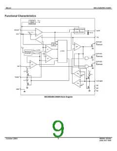
Input Undervoltage Lockout
The MIC2586/MIC2586R have an internal undervoltage
lockout circuit that inhibits operation of the controller’s
internal circuitry unless the power supply voltage is stable
and within an acceptable tolerance. If the supply voltage to
the controller with respect to ground is greater than the VUVH
threshold voltage (8V typical), the controller’s internal circuits
are enabled and the controller is then ready for normal
operation pending the state of the ON pin voltage. Once in
steady-state operation, the controller’s internal circuits
remain active so long as the supply voltage with respect to
ground is higher than the controller’s internal VUVL threshold
voltage (7.5V typical).
CPG
tPG(1−3)
=
× VPG3
ICPG
where VPG3 (1.25V, typically) is the PWRGD3 (or /PWRGD3)
threshold voltage for PGTIMER. Therefore, PWRGD2 (or
/PWRGD2) will be delayed after the assertion of PWRGD1
(or /PWRGD1) by:
tPG(1−2)(ms) ≅ 90 × CPG(µF)
(8)
PWRGD3 (/PWRGD3) follows the assertion of PWRGD1
(/PWRGD1) by a delay:
tPG(1−3) (ms) ≅ 180 × CPG (µF)
(9)
For example, for a CPG of 0.1µF, PWRGD2 (or /PWRGD2)
will be asserted 9ms after PWRGD1 (or /PWRGD1).
PWRGD3 (or /PWRGD3) will then be asserted 9ms after
PWRGD2 (or /PWRGD2) and 18ms after the assertion of
Power-is-Good Output Signals
For the MIC2586-1/MIC2586R-1, power-good output signal
PWRGD1 will be high impedance when the FB pin voltage is
higher than the VFBH threshold and will pull down to GND
when the FB pin voltage is lower than the VFBL threshold. For
the MIC2586-2/MIC2586R-2, power-good output signal
/PWRGD1 will pull down to GND when the FB pin voltage is
higher than the VFBH threshold and will be high impedance
when the FB pin voltage is lower than the VFBL threshold.
Hence, the (-1) parts have an active-HIGH PWRGDx signal
and the (-2) parts have an active-LOW /PWRGDx output.
PWRGDx (or /PWRGDx) may be used as an enable signal
for one or more DC/DC converter modules or for other
system functions. When used as an enable signal, the time
necessary for the PWRGDx (or /PWRGDx) signal to pull-up
(when in high impedance state) will depend upon the (RC)
load at the respective Power-is-Good pin.
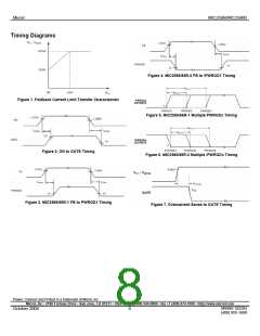
PWRGD1 (or /PWRGD1). The relationships between VOUT
,
VFBH, PWRGD1, PWRGD2, and PWRGD3 are shown in
Figures 5 and 6.
Each Power-is-Good output pin is connected to an open-
drain, N-channel transistor implemented with high-voltage
structures. These transistors are capable of operating with
pull-up resistors to supply voltages as high as 100V.
M9999-102204
(408) 955-1690
October 2004
12

 MICREL [ MICREL SEMICONDUCTOR ]