Micrel
MIC2586/MIC2586R
choice for an 18-V Zener diode in this application is the
MMSZ5248B, available in a small SOD123 package.
Functional Description
Hot Swap Insertion
CGATE is used to adjust the GATE voltage slew rate while R3
minimizes the potential for high-frequency parasitic
oscillations from occurring in M1. However, note that
resistance in this part of the circuit has a slight destabilizing
effect upon the MIC2586/MIC2586R's current regulation
loop. Compensation resistor R4 is necessary for stabilization
of the current regulation loop. The current through the power
transistor during initial inrush is given by:
When circuit boards are inserted into systems carrying live
supply voltages ("hot swapped"), high inrush currents often
result due to the charging of bulk capacitance that resides
across the circuit board's supply pins. These current spikes
can cause the system's supply voltages to temporarily go out
of regulation causing data loss or system lock-up. In more
extreme cases, the transients occurring during a hot swap
event may cause permanent damage to connectors or on-
board components.
IGATEON
IINRUSH = CLOAD
×
(2)
CGATE
The MIC2586/MIC2586R is designed to address these
issues by limiting the maximum current that is allowed to flow
during hot swap events. This is achieved by implementing a
constant-current control loop at turn-on. In addition to inrush
current control, the MIC2586 and MIC2586R incorporate
input voltage supervisory functions and user-programmable
overcurrent protection, thereby providing robust protection for
both the system and the circuit board.
The drain current of the MOSFET is monitored via an
external current sense resistor to ensure that it never
exceeds the programmed threshold, as described in the
"Circuit Breaker Operation" section.
A capacitor connected to the controller’s TIMER pin sets the
value of overcurrent detector delay, tFLT, which is the time for
which an overcurrent event must last to signal a fault
condition and to cause an output latch-off. These devices will
be driving a capacitive load in most applications, so a
properly chosen value of CTIMER prevents false-, or nuisance-,
tripping at turn-on as well as providing immunity to noise
spikes after the start-up cycle is complete. The procedure for
selecting a value for CTIMER is given in the "Circuit Breaker
Operation" section.
Input Supply Transient Suppression and Filtering
The MIC2586/MIC2586R is guaranteed to withstand
transient voltage spikes up to 100V. However, voltage
spikes in excess of 100V may cause damage to the
controller.
In order to suppress transients caused by
parasitic inductances, wide (and short) power traces should
be utilized. Alternatively, a heavier trace plating will help
minimize inductive spikes that may arise during events (e.g.,
short circuit loads) that can cause a large di/dt to occur.
External surge protection, such as a clamping diode, is also
recommended as an added safeguard for device (and
system) protection. Lastly, a 0.1µF filter capacitor is
recommended to help reject additional noise.
Overcurrent Protection
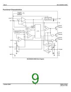
The MIC2586 and the MIC2586R use an external, low-value
resistor in series with the drain of the external MOSFET to
measure the current flowing into the load. The VCC
connection (Pin 14) and the SENSE connection (Pin 13) are
the (+) and (-) inputs, respectively, of the device's internal
current sensing circuits. Kelvin sense connections are
strongly recommended for sensing the voltage across these
pins. See the “Applications Information” for further details.
Start-Up Cycle
When the power supply voltage to the MIC2586/MIC2586R is
higher than the VUVH and the VONH threshold voltages, a start
cycle is initiated. When the controller is enabled, an internal
16µA current source (IGATEON) is enabled and the GATE pin
voltage rises from 0V with respect to ground at a rate equal
to:
The nominal current limit is determined by the following
equation.
VTRIP(TYP)
ILIMIT
=
(3)
RSENSE
where VTRIP(TYP) is the typical current limit threshold specified
in the datasheet and RSENSE is the value of the selected
sense resistor. As the MIC2586 and the MIC2586R employ
a constant-current regulation scheme in current limit, the
charge pump’s output voltage at the GATE pin is adjusted so
that the voltage across the external sense resistor is held
equal to VTRIP while the capacitor connected to the TIMER
pin is being charged. If the current-limit condition goes away
before the TIMER pin voltage rises above the VTIMERH
threshold, then steady-state operation resumes. To prevent
excessive power dissipation in the external MOSFET under
load current fault conditions, the FB pin voltage is used as
dVGATE IGATEON
=
(1)
dt
CGATE
The internal charge pump has sufficient output drive to fully
enhance commonly available power MOSFETs for the lowest
possible DC losses. The gate drive is guaranteed to be
between 7.5V and 18V over the entire supply voltage
operating range (10V to 80V), so 60V BVDSS and 30V BVDSS
N-channel power MOSFETs can be used for +48V and +24V
applications, respectively. However, an external Zener diode
(18-V) connected from the source to the gate as shown in the
"Typical Applications" circuit is highly recommended. A good
M9999-102204
(408) 955-1690
October 2004
10

 MICREL [ MICREL SEMICONDUCTOR ]