Micrel
MIC2589/MIC2595
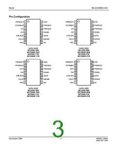
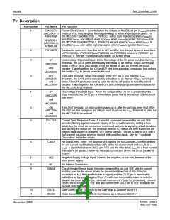
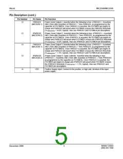
Pin Description
Pin Number
Pin Name
Pin Function
Power-Good Output 1: Asserted when the voltage on the DRAIN pin (VDRAIN) is within
PGTH of VEE, indicating that the output voltage is within proper specifications. For
the MIC2589-1 and MIC2595-1, PWRGD1 will be high impedance when VDRAIN is
less than VPGTH, and will pull-down to VDRAIN when VDRAIN is greater than VPGTH. For
the MIC2589-2 and MIC2595-2, /PWRGD1 will pull-down to VDRAIN when VDRAIN is
1
PWRGD1
(MIC25XX-1)
Active High
V
/PWRGD1
(MIC25XX-2)
Active Low
less than VPGTH, and will be high-impedance when VDRAIN is greater than VPGTH
.
2
3
PGTIMER
A capacitor connected from this pin to VEE sets the time interval between assertions
of PWRGD2 (or /PWRGD2) and PWRGD3 (or /PWRGD3) relative to PWRGD1 (or
/PWRGD1). See the “Functional Description” for further detail.
UV
Undervoltage Threshold Input: When the voltage at the UV pin is less than the VUVL
threshold, the GATE pin is immediately pulled low by an internal 100µA current pull-
down. The UV pin is also used to cycle the device off and on to reset the circuit
breaker. Taken together, the OV and UV pins form a window comparator that defines
the limits of VEE to deliver power to the load.
(MIC2589
and
MIC2589R)
3
4
OFF
(MIC2595
and
Turn-Off Threshold: When the voltage at the OFF pin is less than the VOFFL
threshold, the GATE pin is immediately pulled low by an internal 100µA current pull-
down. The OFF pin is also used to cycle the device off and on to reset the circuit
breaker. Taken together, the ON and OFF pins provide programmable hysteresis for
the MIC2595 to be enabled.
MIC2595R)
OV
(MIC2589
and
Overvoltage Threshold Input: When the voltage at the OV pin is greater than the
V
OVH threshold, the GATE pin is immediately pulled low by an internal 100µA current
pull-down.
MIC2589R)
4
5
ON
(MIC2595
and
Turn-On Threshold: At initial system power-up or after the part has been shut off by
the OFF pin, the voltage on the ON pin must be above the VONH threshold in order for
the MIC2595 to be enabled.
MIC2595R)
CFILTER
Current Limit Response Timer: A capacitor connected between this pin and VEE
provides filtering against nuisance tripping of the circuit breaker by setting a time
delay, tFLT, for which an overcurrent event must last prior to signaling a fault condition
and latching the output off. The minimum time for tFLT will be the time it takes for the
output (capacitance) to charge to VEE during start-up. This pin is held to VEE with a
3µA current pull-down when no current limit condition exists. See the “Functional
Description” for further details.
6
7
CNLD
VEE
No-Load Detect Timer: The absence of a load for the MIC2589/MIC2589R is defined
for any current load that is less than 20% of the full-scale current limit (i.e., 0.20 ×
I
LIM). A capacitor between CNLD and VEE sets the filter delay, tNLD, for a load current
that is 80% (or greater) below the full-scale current limit before the circuit breaker is
tripped.
Negative Supply Voltage Input: Connect the negative, or low side, terminal of the
input power supply.
8
9
NC
No Internal Connection
SENSE
Circuit Breaker Sense Input: A resistor between this pin and VEE sets the current
limit trip point for the circuit. When the current limit threshold of IR = 50mV is
exceeded for tFLT, the circuit breaker is tripped and the GATE pin is immediately
pulled low by IGATEOFF. Toggling UV or OV will reset the circuit breaker. In order to
disable the circuit breaker (i.e., eliminate overcurrent VSENSE-VEE protection), connect
(short) the SENSE pin to VEE and also connect the CNLD pin to VEE to disable the
no-load detection feature.
10
11
GATE
Gate Drive Output: Connects to the Gate of an N-Channel MOSFET.
Drain Sense Input: Connects to the Drain of an N-Channel MOSFET.
DRAIN
4
M9999-120505
(408) 955-1690
December 2005

 MICREL [ MICREL SEMICONDUCTOR ]