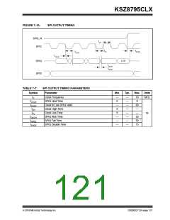
KSZ8795CLX
8.0
RESET CIRCUIT
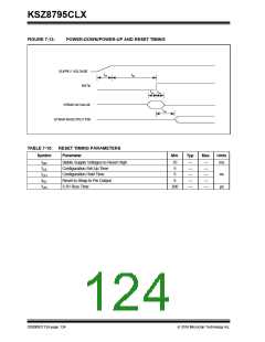
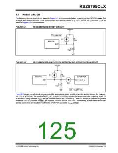
The following discrete reset circuit, shown in Figure 8-1, is recommended when powering up the KSZ8795 device. For
an application where the reset circuit signal comes from another device (e.g., CPU, FPGA, etc.), the reset circuit as
shown in Figure 8-2 is recommended.
FIGURE 8-1:
RECOMMENDED RESET CIRCUIT
VDDIO
D1: 1N4148
R
D1
10k
KS8795
RST
C
10µF
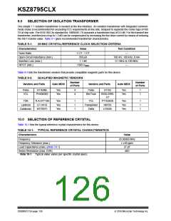
FIGURE 8-2:
RECOMMENDED CIRCUIT FOR INTERFACING WITH CPU/FPGA RESET
VDDIO
R
D1
10k
KS8795
CPU/FPGA
RST
RST_OUT_n
D2
C
10µF
D1, D2: 1N4148
Figure 8-2 shows a reset circuit recommended for applications where reset is driven by another device (for example,
the CPU or an FPGA). The reset out RST_OUT_n from CPU/FPGA provides the warm reset after power up reset. D2
is required if using different VDDIO voltage between switch and CPU/FPGA. Diode D2 should be selected to provide
maximum 0.3V VF (Forward Voltage), for example, VISHAY BAT54, MSS1P2L. Alternatively, a level shifter device can
also be used. D2 is not required if switch and CPU/FPGA use same VDDIO voltage.
2016 Microchip Technology Inc.
DS00002112A-page 125

 MICREL [ MICREL SEMICONDUCTOR ]