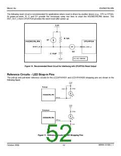
Micrel, Inc.
KSZ9021RL/RN
Timing Diagrams
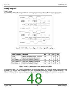
RGMII Timing
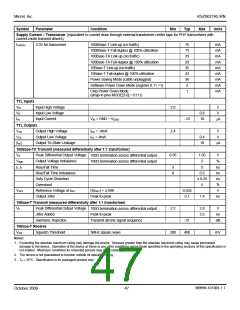
The KSZ9021RL/RN RGMII timing conforms to the timing requirements per the RGMII Version 1.3 Specification.
Figure 5. RGMII v1.3 Specification (Figure 2 – Multiplexing and Timing Diagram)
Timing Parameter
TskewT
Description
Min
-500
1
Typ
Max
500
2.6
8.8
Unit
ps
Data to Clock output Skew (at Transmitter)
Data to Clock input Skew (at Receiver)
Clock Cycle Duration for 1000Base-T
TskewR
ns
Tcyc (1000Base-T)
7.2
36
8
ns
Tcyc (100Base-TX) Clock Cycle Duration for 100Base-TX
Tcyc (10Base-T) Clock Cycle Duration for 10Base-T
40
44
ns
360
400
440
ns
Table 10. RGMII v1.3 Specification (Timing Specifics from Table 2)
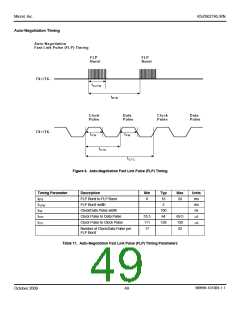
Accounting for TskewT, the TskewR specification in the above table requires the PCB board design to incorporate clock
routing for TXC and RXC with an additional trace delay of greater than 1.5ns and less than 2.1ns for 1000Base-T. For
10Base-T/100Base-TX, the maximum delay is much greater than the 2.1ns for 1000Base-T, and thus is not specified.
M9999-101309-1.1
October 2009
48

 MICREL [ MICREL SEMICONDUCTOR ]