Datasheet Version1.1
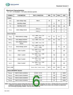
Electrical Characteristics
Ta = 25℃, CS Resistance = 6.8Ω unless otherwise specified
SYMBOL
Supply
VVIN
PARAMETER
TEST CONDITION
MIN
TYP
MAX
UNIT
Input voltage range
Operating voltage
Operating current
Note 6
50
700
V
V
VVCC
-
15
465
12
-
Iop
210
720
uA
V
UVLO_H
UVLO_L
-
-
-
-
VUVLO
Under voltage lockout
10
V
Driver Section
VVIN = 200V, VGND = 0V
VMODE = open
VRhold
Rhold reference voltage
Over voltage protection
4.5
5.2
5.9
V
V
V
OVP_H
OVP_L
VVIN = 200V, VGND = 0V
VVIN = 200V, VGND = 0V
12.2
13.5
13.2
14.8
Over voltage protection
release
VVIN = 200V, VGND = 0V,
VOUT0~3 = 400V
ID Leak
IOUT0
Driver leakage current
Driver 0 current
Driver 1 current
Driver 2 current
Driver 3 current
-
-
10
uA
mA
mA
mA
mA
mA
VVIN =200V, VOUT0 = 40V
VRhold = 0V
-
85
-
VVIN =200V, VOUT1 = 40V
VRhold = 0V
IOUT1
-
130
155
185
555
-
VVIN =200V, VOUT2 = 40V
VRhold = 0V
IOUT2
-
-
-
-
VVIN =200V, VOUT3 = 40V
VRhold = 0V
IOUT3
IOUT_SUM
IOUT0 + IOUT1 + IOUT2 + IOUT3
527.5
587.5
Internal MOSFET Section
RDS(ON)1
RDS(ON)2
RDS(ON)3
RDS(ON)4
Drain to source resistance
Vd=30V, Vs=0V
Vd=30V, Vs=0V
Vd=30V, Vs=0V
Vd=30V, Vs=0V
255
130
130
131
mohm
mohm
mohm
mohm
Drain to source resistance
Drain to source resistance
Drain to source resistance
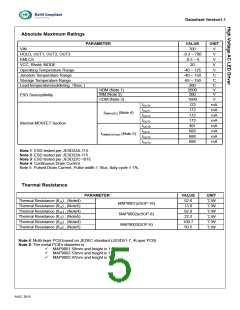
Note 6: Stress beyond the maximum ratings listed above may incur permanent damage to the device. Operating above the recommended
conditions for extended time may stress the device and affect device reliability.Also the device may not operate normally above
the recommended operating conditions. These are stress ratings only.
AUG. 2015

 MGCHIP [ MagnaChip ]