Datasheet Version1.1
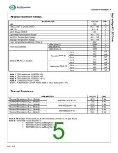
Absolute Maximum Ratings
PARAMETER
VALUE
700
UNIT
V
VIN
HOLD, OUT1, OUT2, OUT3
EMI,CS
-0.3 ~ 700
-0.3 ~ 6
20
V
V
VCC, Rhold, MODE
V
Operating Temperature Range
Junction Temperature Range
Storage Temperature Range
Lead temperature(soldering, 10sec )
-40 ~ 125
-40 ~ 150
℃
℃
-65 ~ 150
260
℃
℃
V
HBM (Note 1)
MM (Note 2)
2000
200
V
ESD Susceptibility
CDM (Note 3)
1000
V
IOUT0
IOUT1
IOUT2
IOUT3
IOUT0
IOUT1
IOUT2
IOUT3
123
172
172
172
491
688
688
688
mA
mA
mA
mA
mA
mA
mA
mA
IDMAX(DC) (Note 4)
Internal MOSFET Section
IDMMAX(Pulse) (Note 5)
Note 1: ESD tested per JESD22A-114.
Note 2: ESD tested per JESD22A-115.
Note 3: ESD tested per JESD22C-101E
Note 4: Continuous Drain Current
Note 5: Pulsed Drain Current, Pulse width ≤ 10us, duty cycle ≤ 1%,
Thermal Resistance
PARAMETER
VALUE
52.6
UNIT
Thermal Resistance (θJA) , (Note4)
℃/W
℃/W
℃/W
℃/W
℃/W
℃/W
MAP9001(eSOP-16)
MAP9002(eSOP-8)
MAP9003(SOP-8)
Thermal Resistance (θJT) , (Note5)
Thermal Resistance (θJA) , (Note4)
Thermal Resistance (θJT) , (Note5)
Thermal Resistance (θJA) , (Note4)
Thermal Resistance (θJT) , (Note5)
13.0
62.8
22.2
100.7
50.5
Note 4: Multi-layer PCB based on JEDEC standard (JESD51-7, 4Layer PCB)
Note 5: The metal PCB’s diameter is
MAP9001 50mm and height is 1.6t.
MAP9002 53mm and height is 1.6t.
MAP9003 47mm and height is 1.6t.
AUG. 2015

 MGCHIP [ MagnaChip ]