(1,0,1): select AIN5 (P1.5) as the analog input
(1,1,0): select AIN6 (P1.6) as the analog input
(1,1,1): select AIN7 (P1.7) as the analog input
AUXR (Address=8EH, Auxiliary Register, Reset Value=0000,xx0xB)
7
6
5
4
3
2
1
0
-
URTS
ADRJ
P41ALE P35ALE
-
-
EXTRAM
ADRJ:
0: The most significant 8 bits of conversion result are saved in ADCH[7:0], while the least significant 2 bits in
ADCL[1:0].
1: The most significant 2 bits of conversion result are saved in ADCH[1:0], while the least significant 8 bits in
ADCL[7:0].
If ADRJ=0
ADCH (Address=C6H, ADC Result High-byte Register, Reset Value=xxH)
7
6
5
4
3
2
1
0
(B9)
(B8)
(B7)
(B6)
(B5)
(B4)
(B3)
(B2)
ADCL (Address=BEH, ADC Result Low-byte Register, Reset Value=xxH)
7
6
5
4
3
2
1
0
(B1)
(B0)
-
-
-
-
-
-
If ADRJ=1
ADCH (Address=C6H, ADC Result High-byte Register, Reset Value=xxH)
7
6
5
4
3
2
1
0
(B9)
(B8)
-
-
-
-
-
-
ADCL (Address=BEH, ADC Result Low-byte Register, Reset Value=xxH)
7
6
5
4
3
2
1
0
(B7)
(B6)
(B5)
(B4)
(B3)
(B2)
(B1)
(B0)
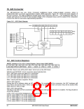
16.2 ADC Operation
For consideration of pin-compatible with the standard 8051 MCU, the ADC hardware cannot have separated
input pins for internal positive (Vref+) and negative (Vref-) reference voltages. The Vref+ and Vref- inputs have
been internally tied to VDD pin and ground, respectively. So, the full-scale voltage Vref+ – Vref- becomes VDD.
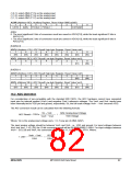
The A/D conversion result can be calculated from the following formula:
x
Vin Vref-
AIN Analog Input Voltage
-
1024 x
=
ADC Result =
VDD Voltage
Vref+ Vref-
-
Where, Vin is the analog input voltage and x = 0~7 (any pin of AIN0~AIN7).
The input analog voltage should be between Vref+ and Vref-, i.e., VDD and ground. For input voltages between
Vref- and Vref- + 1/2 LSB, the 10-bit conversion result will be 00,0000,0000B = 000H. For input voltages between
Vref+ – 3/2 LSB and Vref+, the conversion result will be 11,1111,1111B = 3FFH. Where:
Vref+ Vref-
VDD
1024
-
1 LSB =
=
1024
MEGAWIN
MPC82G516A Data Sheet
82

 MEGAWIN [ MEGAWIN TECHNOLOGY CO., LTD ]