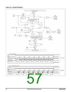
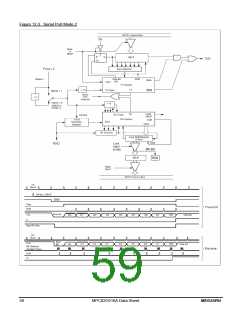
12.1.5 More About Mode 0
Serial data enters and exits through RXD. TXD outputs the shift clock. 8 bits are transmitted/received: 8 data bits
(LSB first). The baud rate is fixed at 1/12 the system clock frequency. Figure 12-1 shows a simplified functional
diagram of the serial port in Mode 0, and associated timing.
Transmission is initiated by any instruction that uses SBUF as a destination register. The “write to SBUF” signal
also loads a 1 into the 9th position of the transmit shift register and tells the TX Control block to commence a
transmission. The internal timing is such that appropriate time will elapse between “write to SBUF” and activation
of Send.
Send enables the output of the shift register to the alternate output function line of P3.0 and also enable Shift
Clock to the alternate output function line of P3.1. Shift Clock is low for 6 clocks, and high for 6 clocks. At every
12-clock cycle the Send is active, the contents of the transmit shift are shifted to the right one position.
As data bits shift out to the right, zeros come in from the left. When the MSB of the data byte is at the output
position of the shift register, then the ‘1’ that was initially loaded into the 9th position, is just to the left of the MSB,
and all positions to the left of that contain zeros. This condition flags the TX Control block to do one last shift and
then deactivate Send and set TI. Both of these actions occur at the 10th bit duration after “write to SBUF.”
Reception is initiated by the condition REN=1 and RI=0. At the next instruction cycle, the RX Control unit writes
the bits 11111110 to the receive shift register, and in the next clock phase activates Receive.
Receive enables Shift Clock to the alternate output function of P3.1 pin. Shift Clock makes transitions every 6
clock cycles. When Receive is active, the contents of the receive shift register are shifted to the left one position.
The value that comes in from the right is the value that was sampled at the P3.0 pin.
As data bits come in from the right, 1s shift out to the left. When the 0 that was initially loaded into the rightmost
position arrives at the leftmost position in the shift register, it flags the RX Control block to do one last shift and
load SBUF. At the 10th bit duration after the write to SCON that cleared RI, Receive is cleared as RI is set.
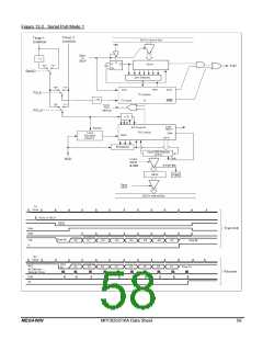
12.1.6 More About Mode 1
10 bits are transmitted through TXD, or received through RXD: a start bit (0), 8 data bits (LSB first), and a stop bit
(1). On receive, the stop bit goes into RB8 in SCON. The baud rate is determined by the Timer 1 or Timer 2
overflow rate. Figure 12-2 shows a simplified functional diagram of the serial port in Mode 1, and associated
timings for transmit/receive.
Transmission is initiated by any instruction that uses SBUF as a destination register. The “write to SBUF” signal
also loads a 1 into the 9th bit position of the transmit shift register and flags the TX Control unit that a
transmission is requested. Transmission actually commences at the instruction cycle following the next rollover in
the divide-by-16 counter. (Thus, the bit times are synchronized to the divide-by-16 counter, not to the “write to
SBUF” signal.)
The transmission begins with activation of Send which puts the start bit at TXD. One bit time later, data is
activated, which enables the output bit of the transmit shift register to TXD. The first shift pulse occurs one bit
time after that.
As data bits shift out to the right, zeros are clocked in from the left. When the MSB of the data byte is at the
output position of the shift register, then the 1 that was initially loaded into the 9th position is just to the left of the
MSB, and all positions to the left of that contain zeros. This condition flags the TX Control unit to do one last shift
and then deactivate Send and set TI. This occurs at the 10th divide-by-16 rollover after “write to SBUF.”
Reception is initiated by a detected 1-to-0 transition at RXD. For this purpose RXD is sampled at a rate of 16
times whatever baud rate has been established. When a transition is detected, the divide-by-16 counter is
immediately reset, and 1FFH is written into the input shift register. Resetting the divide-by-16 counter aligns its
rollovers with the boundaries of the incoming bit times.
The 16 states of the counter divide each bit time into 16ths. At the 7th, 8th, and 9th counter states of each bit
time, the bit detector samples the value of RXD. The value accepted is the value that was seen in at least 2 of the
3 samples. This is done for noise rejection. If the value accepted during the first bit time is not 0, the receive
circuits are reset and the unit goes back to looking for another 1-to-0 transition. This is to provide rejection of
55
MPC82G516A Data Sheet
MEGAWIN

 MEGAWIN [ MEGAWIN TECHNOLOGY CO., LTD ]