MX29LA129M H/L
The single cycle Query command is valid only when the
device is in the Read mode, including Erase Suspend,
Standby mode, and Read ID mode;however, it is ignored
otherwise.
QUERY COMMAND AND COMMON FLASH
INTERFACE (CFI) MODE
MX29LA129M H/L is capable of operating in the CFI mode.
This mode all the host system to determine the manu-
facturer of the device such as operating parameters and
configuration.Two commands are required in CFI mode.
Query command of CFI mode is placed first, then the
Reset command exits CFI mode.These are described in
Table 4.
The Reset command exits from the CFI mode to the
Read mode, or Erase Suspend mode, or read ID mode.
The command is valid only when the device is in the CFI
mode.
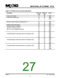
Table 4-1. CFI mode: Identification Data Values
(All values in these tables are in hexadecimal)
Description
Addressh Addressh
Datah
(x16)
10
(x8)
20
22
24
26
28
2A
2C
2E
30
32
34
Query-unique ASCII string "QRY"
0051
0052
0059
0002
0000
0040
0000
0000
0000
0000
0000
11
12
Primary vendor command set and control interface ID code
Address for primary algorithm extended query table
13
14
15
16
Alternate vendor command set and control interface ID code (none)
Address for secondary algorithm extended query table (none)
17
18
19
1A
Table 4-2. CFI Mode: System Interface Data Values
Description
Addressh Addressh
Datah
(x16)
1B
1C
1D
1E
1F
20
(x8)
36
VCC supply, minimum (2.7V)
0027
0036
0000
0000
0007
0007
000A
0000
0001
0005
0004
0000
VCC supply, maximum (3.6V)
38
VPP supply, minimum (none)
3A
3C
3E
40
VPP supply, maximum (none)
Typical timeout for single word/byte write (2N us)
Typical timeout for maximum size buffer write (2N us)
Typical timeout for individual block erase (2N ms)
Typical timeout for full chip erase (2N ms)
Maximum timeout for single word/byte write times (2N X Typ)
Maximum timeout for maximum size buffer write times (2N X Typ)
Maximum timeout for individual block erase times (2N X Typ)
Maximum timeout for full chip erase times (not supported)
21
42
22
44
23
46
24
48
25
4A
4C
26
P/N:PM1171
REV. 1.0, FEB. 27, 2006
26

 Macronix [ MACRONIX INTERNATIONAL ]