MX29LA129M H/L
mand is written during a programming process, the de-
vice halts the program operation within 15us maximum
(5 us typical) and updates the status bits. Addresses are
not required when writing the Program Suspend com-
mand.
AUTOMATIC CHIP/SECTOR ERASE COM-
MAND
The device does not require the system to preprogram
prior to erase.The Automatic Erase algorithm automati-
cally pre-program and verifies the entire memory for an
all zero data pattern prior to electrical erase.The system
is not required to provide any controls or timings during
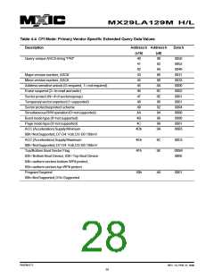
these operations. Table 3 shows the address and data
requirements for the chip erase command sequence.
After the programming operation has been suspended,
the system can read array data from any non-suspended
sector. The Program Suspend command may also be
issued during a programming operation while an erase is
suspended. In this case, data may be read from any
addresses not in Erase Suspend or Program Suspend. If
a read is needed from the Secured Silicon Sector area
(One-time Program area), then user must use the proper
command sequences to enter and exit this region.
Any commands written to the chip during the Automatic
Erase algorithm are ignored. Note that a hardware reset
during the chip erase operation immediately terminates
the operation.The Chip Erase command sequence should
be reinitiated once the device has returned to reading
array data, to ensure data integrity.
The system may also write the autoselect command
sequence when the device is in the Program Suspend
mode. The system can read as many autoselect codes
as required.When the device exits the autoselect mode,
the device reverts to the Program Suspend mode, and
is ready for another valid operation. See Autoselect Com-
mand Sequence for more information.
The system can determine the status of the erase op-
eration by using Q7, Q6, Q2, or RY/BY#.See "Write Op-
eration Status" for information on these status bits.When
the Automatic Erase algorithm is complete, the device
returns to reading array data and addresses are no longer
latched.
After the Program Resume command is written, the de-
vice reverts to programming.The system can determine
the status of the program operation using the Q7 or Q6
status bits, just as in the standard program operation.
See Write Operation Status for more information.
Figure 10 illustrates the algorithm for the erase opera-
tion. See the Erase/Program Operations tables in "AC
Characteristics" for parameters, and to Figure 9 for tim-
ing diagrams.
SETUP AUTOMATIC CHIP/SECTOR ERASE
Chip erase is a six-bus cycle operation. There are two
"unlock" write cycles. These are followed by writing the
"set-up" command 80H. Two more "unlock" write cycles
are then followed by the chip erase command 10H, or
the sector erase command 30H.
The MX29LA129M H/L contains a Silicon-ID-Read op-
eration to supplement traditional PROM programming
methodology. The operation is initiated by writing the read
silicon ID command sequence into the command regis-
ter. Following the command write, a read cycle with
A2=VIL,A1=VIL retrieves the manufacturer code.A read
cycle with A2=VIL, A1=VIH returns the device code.
P/N:PM1171
REV. 1.0, FEB. 27, 2006
24

 Macronix [ MACRONIX INTERNATIONAL ]