MX29LA129M H/L
but not within VSS±0.3V, the standby current will be
greater.
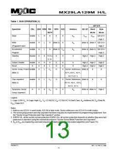
STANDBY MODE
When using both pins of CEx and RESET#, the device
enter CMOS Standby with both pins held atVCC ±0.3V.
If CEx and RESET# are held at VIH, but not within the
range ofVCC ±0.3V, the device will still be in the standby
mode, but the standby current will be larger.During Auto
Algorithm operation,VCC active current (ICC2) is required
even CEx = "H" until the operation is completed. The
device can be read with standard access time (tCE) from
either of these standby modes, before it is ready to read
data.
The RESET# pin may be tied to system reset circuitry.
A system reset would that also reset the Flash memory,
enabling the system to read the boot-up firmware from
the Flash memory.
If RESET# is asserted during a program or erase
operation, the RY/BY# pin remains a "0" (busy) until the
internal reset operation is complete, which requires a time
of tREADY (during Embedded Algorithms).The system
can thus monitor RY/BY# to determine whether the reset
operation is complete. If RESET# is asserted when a
program or erase operation is completed within a time of
tREADY (not during Embedded Algorithms).The system
can read data tRH after the RESET# pin returns to VIH.
AUTOMATIC SLEEP MODE
The automatic sleep mode minimizes Flash device en-
ergy consumption.The device automatically enables this
mode when address remain stable for tACC+30ns. The
automatic sleep mode is independent of the CEx, WE#,
and OE# control signals. Standard address access tim-
ings provide new data when addresses are changed.While
in sleep mode, output data is latched and always avail-
able to the system. ICC4 in the DC Characteristics table
represents the automatic sleep mode current specifica-
tion.
Refer to the AC Characteristics tables for RESET#
parameters and to Figure 3 for the timing diagram.
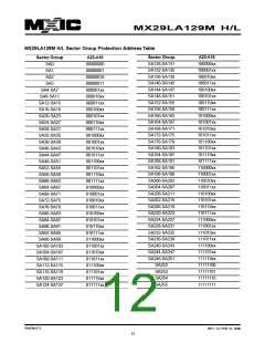
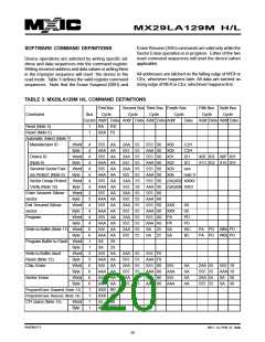
SECTOR GROUP PROTECT OPERATION
The MX29LA129M H/L features hardware sector group
protection. This feature will disable both program and
erase operations for these sector group protected. In
this device, a sector group consists of four adjacent sec-
tors which are protected or unprotected at the same time.
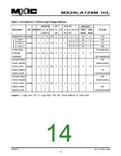
To activate this mode, the programming equipment must
forceVID on address pin A10 and control pin OE#, (sug-
gest VID = 12V) A7 = VIL and CEx = VIL. (see Table 2)
Programming of the protection circuitry begins on the
falling edge of the WE# pulse and is terminated on the
rising edge. Please refer to sector group protect algo-
rithm and waveform.
OUTPUT DISABLE
With the OE# input at a logic high level (VIH), output
from the devices are disabled.This will cause the output
pins to be in a high impedance state.
RESET# OPERATION
MX29LA129M H/L also provides another method.Which
requires VID on the RESET# only. This method can be
implemented either in-system or via programming equip-
ment. This method uses standard microprocessor bus
cycle timing.
The RESET# pin provides a hardware method of resetting
the device to reading array data.When the RESET# pin
is driven low for at least a period of tRP, the device
immediately terminates any operation in progress,
tristates all output pins, and ignores all read/write
commands for the duration of the RESET# pulse. The
device also resets the internal state machine to reading
array data.The operation that was interrupted should be
reinitiated once the device is ready to accept another
command sequence, to ensure data integrity
To verify programming of the protection circuitry, the pro-
gramming equipment must forceVID on address pin A10
( with CEx and OE# at VIL and WE# at VIH). When
A2=1, it will produce a logical "1" code at device output
Q0 for a protected sector. Otherwise the device will pro-
duce 00H for the unprotected sector. In this mode, the
addresses, except for A2, are don't care. Address loca-
tions with A2 = VIL are reserved to read manufacturer
and device codes. (Read Silicon ID)
Current is reduced for the duration of the RESET# pulse.
When RESET# is held at VSS±0.3V, the device draws
CMOS standby current (ICC4).If RESET# is held atVIL
P/N:PM1171
REV. 1.0, FEB. 27, 2006
16

 Macronix [ MACRONIX INTERNATIONAL ]