MX26L3220
REVISION HISTORY
Revision No. Description
Page
P1,7
P5
Date
JUL/23/2001
0.1
1.To added the VI/O voltage range and performance
2.To modify Autoselect code table
3.To added Deep power-down mode
P9,10
P23
P24
P2
P1,2,35
P1
4.To added chip erase algorithm flowchart
5.To added secured silicon sector protect Algorithm flowchart
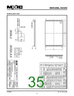
6.To modify the 14-pin of 48 TSOP package from NC to VCC
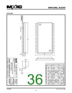
1.To added 44 SOP package
2.To modify the VI/O range from 1.8V~5V to 1.8V~3.6V
3.Cancel th regulated voltage range
0.2
0.3
JUL/31/2001
SEP/26/2001
14
4.Modify DC Characteristics table for VIL/VIH voltage when VI/O range P15
is 1.8V~2.6V
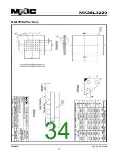
1.To Added 0.8mm ball pitch 48 ball CSP package
2.To modify VI/O voltage range from 1.8V to 1.65V
3.To modify ICC4/tCS/tCH/tOLZ/tWHGL spec
4.To modify VCC standby current from 50uA to 30uA
5.Cancel the deep power-down mode
P2,34
P1,8,15
P15,17
P1,16
P11,16
P1,31
P1,31
P2
6.To modify the programming time
0.4
0.5
1.To modify chip erase time from 45ns(typ.) to 90ns
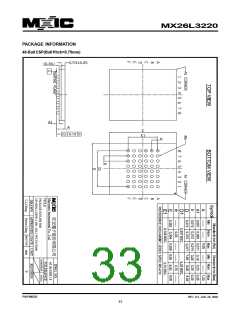
2.To modify the CSP size from 8mm x 9mm to 9mm x 8mm
3.To modify the ICC1 @5MHz:9/16mA-->17/25mA
ICC1 @1MHz:2/4mA-->4/7mA
NOV/27/2001
JAN/29/2002
P15
4. To correct the VHH to 12V±0.5V
P15
1.To modify the content error
P1,7,11
P/N:PM0826
REV. 0.5, JAN. 29, 2002
37

 Macronix [ MACRONIX INTERNATIONAL ]