MX26L3220
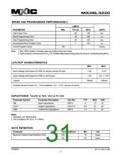
ERASE AND PROGRAMMING PERFORMANCE(1)
LIMITS
PARAMETER
MIN.
TYP.(2)
MAX.
180
UNITS
sec
Chip Erase Time
90
30
70
7
Word Programming Time
Chip Programming Time
Accelerated Word Program Time
Erase/Program Cycles
350
us
125
sec
210
us
100
Cycles
Note: 1.Not 100% Tested, Excludes external system level over head.
2.Typical values measured at 25°C,3.3V.Additionally programming typicals assume checkerboard pattern.
LATCHUP CHARACTERISTICS
MIN.
-1.0V
MAX.
13.5V
Input Voltage with respect to GND on all pins except I/O pins
Input Voltage with respect to GND on all I/O pins
Current
-1.0V
Vcc + 1.0V
+100mA
-100mA
Includes all pins except Vcc. Test conditions: Vcc = 5.0V, one pin at a time.
CAPACITANCE TA=0°C to 70°C, VCC=2.7V~3.6V
Parameter Symbol
Parameter Description
Input Capacitance
Test Set
VIN=0
TYP
MAX
7.5
12
UNIT
pF
CIN
6
COUT
CIN2
Output Capacitance
Control Pin Capacitance
VOUT=0
VIN=0
8.5
7.5
pF
9
pF
Notes:
1. Sampled, not 100% tested.
2.Test conditions TA=25°C, f=1.0MHz
DATA RETENTION
Parameter
Test Conditions
Min
10
Unit
Minimum Pattern Data Retention Time
150
125
Years
Years
20
P/N:PM0826
REV. 0.5, JAN. 29, 2002
31

 Macronix [ MACRONIX INTERNATIONAL ]