MX26L3220
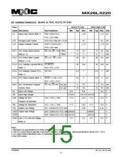
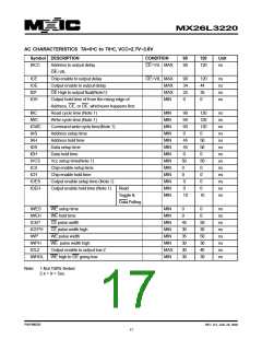
AC CHARACTERISTICS TA=0°C to 70°C, VCC=2.7V~3.6V
Symbol DESCRIPTION
CONDITION
90
120
Unit
tACC
Address to output delay
CE=VIL MAX
90
120
ns
OE=VIL
tCE
tOE
tDF
tOH
Chip enable to output delay
Output enable to output delay
OE High to output float(Note1)
Output hold time of from the rising edge of
Address, CE, or OE, whichever happens first
Read cycle time (Note 1)
Write cycle time (Note 1)
Command write cycle time(Note 1)
Address setup time
OE=VIL MAX
MAX
90
34
25
0
120
44
35
0
ns
ns
ns
ns
MAX
MIN
tRC
MIN
MIN
MIN
MIN
MIN
MIN
MIN
MIN
MIN
MIN
MIN
MIN
MIN
90
90
90
0
120
120
120
0
ns
ns
ns
ns
ns
ns
ns
us
ns
ns
ns
ns
ns
tWC
tCWC
tAS
tAH
Address hold time
45
45
0
50
50
0
tDS
Data setup time
tDH
Data hold time
tVCS
tCS
Vcc setup time(Note 1)
50
0
50
0
Chip enable setup time
tCH
Chip enable hold time
0
0
tOES
tOEH
Output enable setup time (Note 1)
0
0
Output enable hold time (Note 1)
Read
0
0
Toggle &
Data Polling
10
10
tWES
tWEH
tCEP
tCEPH
tWP
WE setup time
MIN
MIN
MIN
MIN
MIN
MIN
MAX
MIN
0
0
ns
ns
ns
ns
ns
ns
ns
ns
WE hold time
0
0
CE pulse width
45
30
35
30
30
30
50
30
50
30
40
30
CE pulse width high
WE pulse width
tWPH
tOLZ
WE pulse width high
Output enable to output low Z
WE high to OE going low
tWHGL
Note: 1.Not 100%Tested
2.tr = tf = 5ns
P/N:PM0826
REV. 0.5, JAN. 29, 2002
17

 Macronix [ MACRONIX INTERNATIONAL ]