MX25L8005
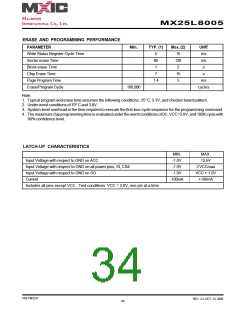
ERASE AND PROGRAMMING PERFORMANCE
PARAMETER
Min.
TYP. (1)
Max.(2)
UNIT
ms
Write Status Register Cycle Time
Sector erase Time
Block erase Time
5
60
1
15
120
2
ms
s
Chip Erase Time
7
15
5
s
PageProgramTime
Erase/ProgramCycle
1.4
ms
100,000
cycles
Note:
1. Typical program and erase time assumes the following conditions: 25° C, 3.3V, and checker board pattern.
2. Under worst conditions of 70°C and 3.0V.
3. System-level overhead is the time required to execute the first-bus-cycle sequence for the programming command.
4. Themaximumchipprogrammingtimeisevaluatedundertheworstconditionsof0C, VCC=3.0V, and100Kcyclewith
90% confidence level.
LATCH-UP CHARACTERISTICS
MIN.
-1.0V
MAX.
12.5V
Input Voltage with respect to GND on ACC
Input Voltage with respect to GND on all power pins, SI, CS#
Input Voltage with respect to GND on SO
-1.0V
2 VCCmax
VCC + 1.0V
+100mA
-1.0V
Current
-100mA
Includes all pins except VCC. Test conditions: VCC = 3.0V, one pin at a time.
P/N:PM1237
REV. 2.2, OCT. 23, 2008
34

 Macronix [ MACRONIX INTERNATIONAL ]