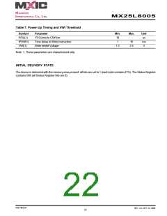
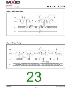
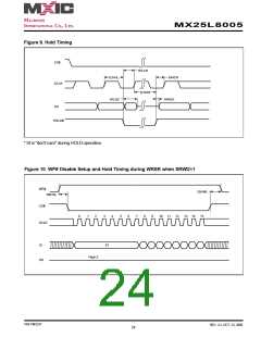
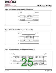
PDF
最近搜索
热门搜索
发布采购

| 型号: | MX25L8005M2C-15G |
| PDF下载: | 下载PDF文件 查看货源 |
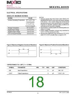
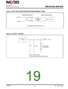
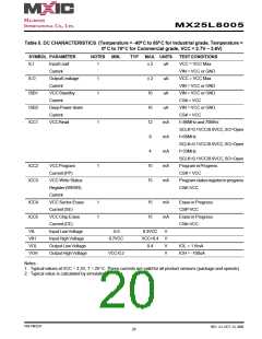
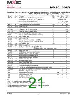
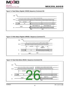
| 内容描述: | 8M - BIT [ ×1 ] CMOS串行闪存 [8M-BIT [x 1] CMOS SERIAL FLASH] |
| 分类和应用: | 闪存存储内存集成电路光电二极管时钟 |
| 文件页数/大小: | 44 页 / 829 K |
| 品牌: |  Macronix [ MACRONIX INTERNATIONAL ] Macronix [ MACRONIX INTERNATIONAL ] |
专业IC领域供求交易平台:提供全面的IC Datasheet资料和资讯,Datasheet 1000万数据,IC品牌1000多家。