MX25L12835F
2. GENERAL DESCRIPTION
MX25L12835F is 128Mb bits serial Flash memory, which is configured as 16,777,216 x 8 internally. When it is in
two or four I/O mode, the structure becomes 67,108,864 bits x 2 or 33,554,432 bits x 4. MX25L12835F feature a
serial peripheral interface and software protocol allowing operation on a simple 3-wire bus while it is in single I/O
mode. The three bus signals are a clock input (SCLK), a serial data input (SI), and a serial data output (SO). Serial
access to the device is enabled by CS# input.
When it is in two I/O read mode, the SI pin and SO pin become SIO0 pin and SIO1 pin for address/dummy bits in-
put and data output. When it is in four I/O read mode, the SI pin, SO pin, WP# and RESET# pin become SIO0 pin,
SIO1 pin, SIO2 pin and SIO3 pin for address/dummy bits input and data output.
The MX25L12835F MXSMIO (Serial Multi I/O) provides sequential read operation on whole chip.
After program/erase command is issued, auto program/erase algorithms which program/erase and verify the speci-
fied page or sector/block locations will be executed. Program command is executed on byte basis, or page (256
bytes) basis, or word basis for erase command is executed on sector (4K-byte), block (32K-byte), or block (64K-byte),
or whole chip basis.
To provide user with ease of interface, a status register is included to indicate the status of the chip. The status read
command can be issued to detect completion status of a program or erase operation via WIP bit.
Advanced security features enhance the protection and security functions, please see security features section for
more details.
When the device is not in operation and CS# is high, it is put in standby mode.
The MX25L12835F utilizes Macronix's proprietary memory cell, which reliably stores memory contents even after
100,000 program and erase cycles.
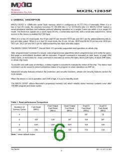
Table 1. Read performance Comparison
Dual Output
Fast Read
(MHz)
Quad Output
Fast Read
(MHz)
Dual IO
Fast Read
(MHz)
Quad IO
Fast Read
(MHz)
Numbers of
Dummy Cycles
Fast Read
(MHz)
4
6
-
-
-
84*
104
104
133
70
104
104*
133
104
104*
133
84
84*
104
133
8
104*
133
10
Note: * mean default status
P/N: PM1795
REV. 1.0, OCT. 23, 2012
6

 Macronix [ MACRONIX INTERNATIONAL ]