MX25L12835F
3V 128M-BIT [x 1/x 2/x 4] CMOS MXSMIO (SERIAL MULTI I/O)
FLASH MEMORY
1. FEATURES
GENERAL
•
•
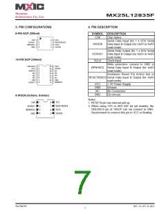
Serial Peripheral Interface compatible -- Mode 0 and Mode 3
Single Power Supply Operation
- 2.7 to 3.6 volt for read, erase, and program operations
128Mb: 134,217,728 x 1 bit structure or 67,108,864 x 2 bits (two I/O mode) structure or 33,554,432 x 4 bits (four
I/O mode) structure
•
•
Protocol Support
- Single I/O, Dual I/O and Quad I/O
•
•
•
Latch-up protected to 100mA from -1V to Vcc +1V
Low Vcc write inhibit is from 2.3V to 2.5V
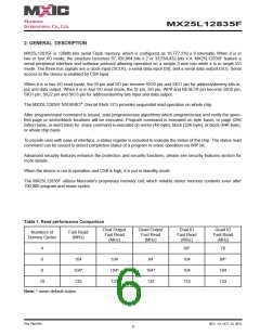
Fast read for SPI mode
- Support clock frequency up to 133MHz for all protocols
- Support Fast Read, 2READ, DREAD, 4READ, QREAD instructions.
- Configurable dummy cycle number for fast read operation
Quad Peripheral Interface (QPI) available
Equal Sectors with 4K byte each, or Equal Blocks with 32K byte each or Equal Blocks with 64K byte each
- Any Block can be erased individually
•
•
•
Programming :
- 256byte page buffer
- Quad Input/Output page program(4PP) to enhance program performance
Typical 100,000 erase/program cycles
20 years data retention
•
•
SOFTWARE FEATURES
•
Input Data Format
- 1-byte Command code
•
Advanced Security Features
- Block lock protection
The BP0-BP3 and T/B status bit defines the size of the area to be protection against program and erase instruc-
tions
- Advanced sector protection function (Solid and Password Protect)
•
Additional 4K bit security OTP
Features unique identifier
factory locked identifiable, and customer lockable
Command Reset
-
-
•
•
•
Program/Erase Suspend and Resume operation
Electronic Identification
JEDEC 1-byte manufacturer ID and 2-byte device ID
- RES command for 1-byte Device ID
-
- REMS command for 1-byte manufacturer ID and 1-byte device ID
Support Serial Flash Discoverable Parameters (SFDP) mode
•
HARDWARE FEATURES
•
SCLK Input
- Serial clock input
P/N: PM1795
REV. 1.0, OCT. 23, 2012
4

 Macronix [ MACRONIX INTERNATIONAL ]