MX25L12835F
9-9. Write Status Register (WRSR)
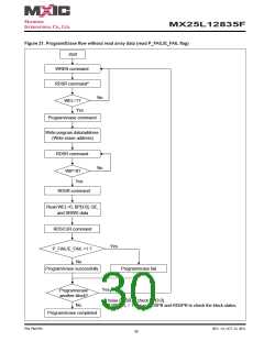
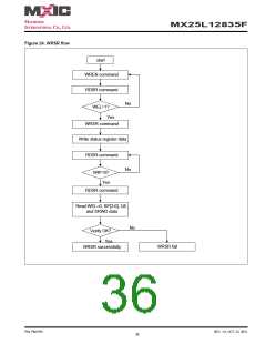
The WRSR instruction is for changing the values of Status Register Bits and Configuration Register Bits. Before
sending WRSR instruction, the Write Enable (WREN) instruction must be decoded and executed to set the Write
Enable Latch (WEL) bit in advance. The WRSR instruction can change the value of Block Protect (BP3, BP2, BP1,
BP0) bits to define the protected area of memory (as shown in "Table 2. Protected Area Sizes"). The WRSR also
can set or reset the Quad enable (QE) bit and set or reset the Status Register Write Disable (SRWD) bit in accord-
ance with Write Protection (WP#/SIO2) pin signal, but has no effect on bit1(WEL) and bit0 (WIP) of the status regis-
ter. The WRSR instruction cannot be executed once the Hardware Protected Mode (HPM) is entered.
The sequence of issuing WRSR instruction is: CS# goes low→ sending WRSR instruction code→ Status Register
data on SI→CS# goes high.
The CS# must go high exactly at the 8 bits or 16 bits data boundary; otherwise, the instruction will be rejected and
not executed. The self-timed Write Status Register cycle time (tW) is initiated as soon as Chip Select (CS#) goes
high. The Write in Progress (WIP) bit still can be check out during the Write Status Register cycle is in progress.
The WIP sets 1 during the tW timing, and sets 0 when Write Status Register Cycle is completed, and the Write En-
able Latch (WEL) bit is reset.
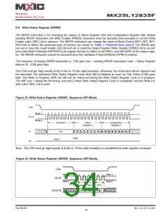
Figure 22. Write Status Register (WRSR) Sequence (SPI Mode)
CS#
0
1
2
3
4
5
6
7
8
9 10 11 12 13 14 15 16 17 18 19 20 21 22 23
Mode 3
Mode 0
SCLK
command
01h
Status
Register In
Configuration
Register In
SI
4
15 14
13
12 11
10 9
8
2
1
0
7
6
5
3
MSB
High-Z
SO
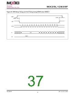
Note : The CS# must go high exactly at 8 bits or 16 bits data boundary to completed the write register command.
Figure 23. Write Status Register (WRSR) Sequence (QPI Mode)
CS#
Mode 3
Mode 0
Mode 3
Mode 0
0
1
2
3
4
5
SCLK
CR in
SR in
Command
01h
H0 L0 H1 L1
SIO[3:0]
P/N: PM1795
REV. 1.0, OCT. 23, 2012
34

 Macronix [ MACRONIX INTERNATIONAL ]