200kHz, 4µA, Rail-to-Rail
I/O Op Amps with Shutdown
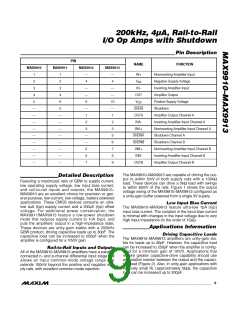
Pin Description
PIN
NAME
FUNCTION
MAX9910
MAX9911
MAX9912
MAX9913
1
2
1
2
—
4
—
4
IN+
Noninverting Amplifier Input
Negative Supply Voltage
Inverting Amplifier Input
V
SS
3
3
—
—
8
—
—
10
—
1
IN-
4
4
OUT
Amplifier Output
5
6
V
Positive Supply Voltage
DD
—
—
—
—
—
—
—
—
—
5
—
1
SHDN
OUTA
INA-
Shutdown
—
—
—
—
—
—
—
—
Amplifier Output Channel A
Inverting Amplifier Input Channel A
Noninverting Amplifier Input Channel A
Shutdown Channel A
2
2
3
3
INA+
—
—
5
5
SHDNA
SHDNB
INB+
6
Shutdown Channel B
7
Noninverting Amplifier Input Channel B
Inverting Amplifier Input Channel B
Amplifier Output Channel B
6
8
INB-
7
9
OUTB
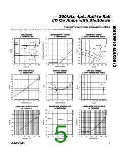
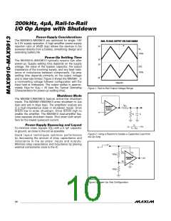
The MAX9910–MAX9913 are capable of driving the out-
put to within 5mV of both supply rails with a 100kΩ
load. These devices can drive a 5kΩ load with swings
to within 60mV of the rails. Figure 1 shows the output
voltage swing of the MAX9910–MAX9913 configured as
a unity-gain buffer powered from a single 3V supply.
Detailed Description
Featuring a maximized ratio of GBW to supply current,
low operating supply voltage, low input bias current,
and rail-to-rail inputs and outputs, the MAX9910–
MAX9913 are an excellent choice for precision or gen-
eral-purpose, low-current, low-voltage, battery-powered
applications. These CMOS devices consume an ultra-
low 4µA (typ) supply current and a 200µV (typ) offset
voltage. For additional power conservation, the
MAX9911/MAX9913 feature a low-power shutdown
mode that reduces supply current to 1nA (typ), and
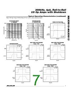
puts the amplifiers’ output in a high-impedance state.
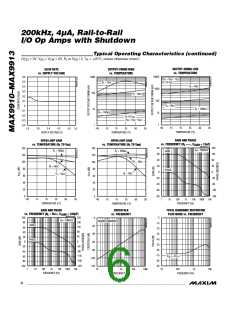
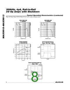
These devices are unity-gain stable with a 200kHz
GBW product, driving capacitive loads up to 30pF. The
capacitive load can be increased to 250pF when the
amplifier is configured for a 10V/V gain.
Low Input Bias Current
The MAX9910–MAX9913 feature ultra-low 1pA (typ)
input bias current. The variation in the input bias current
is minimal with changes in the input voltage due to very
high input impedance (in the order of 1GΩ).
Applications Information
Driving Capacitive Loads
The MAX9910–MAX9913 amplifiers are unity-gain sta-
ble for loads up to 30pF. However, the capacitive load
can be increased to 250pF when the amplifier is config-
ured for a minimum gain of 10V/V. Applications that
require greater capacitive-drive capability should use
an isolation resistor between the output and the capaci-
tive load (Figure 2). Also, in unity-gain applications with
Rail-to-Rail Inputs and Outputs
All of the MAX9910–MAX9913 amplifiers have a parallel-
connected n- and p-channel differential input stage that
allows an input common-mode voltage range that
extends 100mV beyond the positive and negative sup-
ply rails, with excellent common-mode rejection.
relatively small R (approximately 5kΩ), the capacitive
L
load can be increased up to 200pF.
_______________________________________________________________________________________
9

 MAXIM [ MAXIM INTEGRATED PRODUCTS ]