200kHz, 4µA, Rail-to-Rail
I/O Op Amps with Shutdown
Power-Supply Considerations
The MAX9910–MAX9913 are optimized for single 1.8V
to 5.5V supply operation. A high amplifier power-supply
rejection ratio of 95dB (typ) allows the devices to be
powered directly from a battery, simplifying design and
extending battery life.
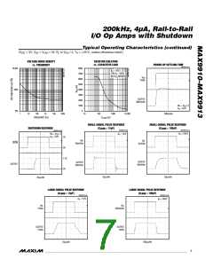
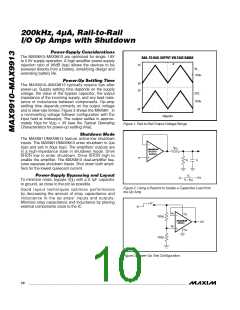
RAIL-TO-RAIL OUTPUT VOLTAGE RANGE
3V
IN_
1V/div
Power-Up Settling Time
The MAX9910–MAX9913 typically require 5µs after
power-up. Supply settling time depends on the supply
voltage, the value of the bypass capacitor, the output
impedance of the incoming supply, and any lead resis-
tance or inductance between components. Op-amp
settling time depends primarily on the output voltage
and is slew-rate limited. Figure 3 shows the MAX991_ in
a noninverting voltage follower configuration with the
input held at midsupply. The output settles in approxi-
0V
3V
OUT_
1V/div
0V
200µs/div
mately 18µs for V
= 3V (see the Typical Operating
DD
Figure 1. Rail-to-Rail Output Voltage Range
Characteristics for power-up settling time).
Shutdown Mode
The MAX9911/MAX9913 feature active-low shutdown
inputs. The MAX9911/MAX9913 enter shutdown in 2µs
(typ) and exit in 30µs (typ). The amplifiers’ outputs are
in a high-impedance state in shutdown mode. Drive
SHDN low to enter shutdown. Drive SHDN high to
enable the amplifier. The MAX9913 dual-amplifier fea-
tures separate shutdown inputs. Shut down both ampli-
fiers for the lowest quiescent current.
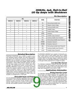
R
ISO
MAX9910–
MAX9913
R
L
C
L
R
Power-Supply Bypassing and Layout
L
A
V
=
≈ 1V/V
R + R
ISO
To minimize noise, bypass V
with a 0.1µF capacitor
L
DD
to ground, as close to the pin as possible.
Figure 2. Using a Resistor to Isolate a Capacitive Load from
the Op Amp
Good layout techniques optimize performance
by decreasing the amount of stray capacitance and
inductance to the op amps’ inputs and outputs.
Minimize stray capacitance and inductance by placing
external components close to the IC.
5.5V
0V
IN-
IN+
V
DD
100kΩ
100kΩ
OUT
MAX991_
V
SS
Figure 3. Power-Up Test Configuration
10 ______________________________________________________________________________________

 MAXIM [ MAXIM INTEGRATED PRODUCTS ]