Smallest TEC Power Drivers for
Optical Modules
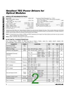
ABSOLUTE MAXIMUM RATINGS
DD
V
to GND..............................................................-0.3V to +6V
Continuous Power Dissipation (T = +70°C)
A
SHDN, MAXV, MAXIP, MAXIN,
CTLI to GND.........................................................-0.3V to +6V
COMP, FREQ, OS1, OS2, CS, REF,
20-Pin 5mm x 5mm x 0.9mm QFN (derate 20.8mW/°C
above +70°C) (Note 2)...................................................1.67W
3mm x 3mm UCSP (derate 22mW/°C
ITEC to GND...........................................-0.3V to (V
+ 0.3V)
+ 0.3V)
above +70°C).................................................................1.75W
Maximum Junction Temperature .....................................+150°C
Storage Temperature Range.............................-65°C to +150°C
Lead Temperature (soldering 10s) ..................................+300°C
DD
DD
PV 1, PV 2 to GND...............................-0.3V to (V
DD
DD
PV 1, PV 2 to V ...........................................-0.3V to +0.3V
DD
DD
DD
PGND1, PGND2 to GND .......................................-0.3V to +0.3V
COMP, REF, ITEC Short to GND ...................................Indefinite
LX Current (Note 1) ........................................ 2.25A LX Current
Stresses beyond those listed under “Absolute Maximum Ratings” may cause permanent damage to the device. These are stress ratings only, and functional
operation of the device at these or any other conditions beyond those indicated in the operational sections of the specifications is not implied. Exposure to
absolute maximum rating conditions for extended periods may affect device reliability.
Note 1: LX has internal clamp diodes to PGND and PVDD. Applications that forward bias these diodes should take care not to exceed
the IC’s package power dissipation limits.
Note 2: Solder underside metal slug to PC board ground plane.
ELECTRICAL CHARACTERISTICS
(V
= PV 1 = PV 2 = SHDN = 5V, 1MHz mode (Note 3). PGND1 = PGND2 = GND, CTLI = MAXV = MAXIP = MAXIN = REF,
DD
DD DD
T
A
= 0°C to +85°C, unless otherwise noted. Typical values at T = +25°C.)
A
PARAMETER
SYMBOL
CONDITIONS
MIN
3.0
TYP
MAX
UNITS
Input Supply Range
V
5.5
V
A
DD
Maximum TEC Current
Reference Voltage
1.5
V
V
V
= 3V to 5.5V, I = 150µA
REF
1.485
1.5
1.2
1.515
5.0
V
REF
DD
DD
Reference Load Regulation
∆V
= 3V to 5V, I = 10µA to 1mA
REF
mV
REF
V
= V
= V
= V
= V
140
40
150
50
160
60
MAXI_
MAXI_
MAXI_
MAXI_
REF
REF
REF
REF
V
V
= 5V
DD
DD
V
V
V
/3
/3
MAXIP/MAXIN Threshold
Accuracy
mV
143
45
150
50
155
55
= 3V
V
V
V
V
V
V
V
V
= 5V, I = 0.2A
= 3V, I = 0.2A
= 5V, I = 0.2A
= 3V, I = 0.2A
0.09
0.11
0.14
0.17
0.03
0.3
0.14
0.16
0.23
0.30
4
DD
DD
DD
DD
LX
NFET On-Resistance
PFET On-Resistance
NFET Leakage
R
Ω
Ω
DS(ON-N)
R
DS(ON-P)
LEAK(N)
= V = 5V, T = +25°C
DD
A
I
µA
µA
= V = 5V, T = +85°C
LX
DD
A
= 0, T = +25°C
0.03
0.3
4
LX
A
PFET Leakage
I
LEAK(P)
= 0, T = +85°C
LX
A
500kHz mode
1MHz mode
500kHz mode
1MHz mode
11
14
21
11
14
3
V
= V
DD
=
REF
COMP
1.500V, V = 5V
16
I
DD(NO
LOAD)
No-Load Supply Current
mA
8
V
= V
DD
=
REF
COMP
1.500V, V = 3.3V
11
Shutdown Supply Current
Thermal Shutdown
I
SHDN = GND, V = 5V (Note 4)
DD
2
mA
DD-SD
T
Hysteresis = 15°C
+165
2.65
2.55
°C
SHUTDOWN
V
V
rising
falling
2.50
2.40
2.80
2.70
DD
DD
UVLO Threshold
V
V
UVLO
2
_______________________________________________________________________________________

 MAXIM [ MAXIM INTEGRATED PRODUCTS ]