Is o la t e d Tra n s fo rm e r Drive r
fo r P CMCIA Ap p lic a t io n s
V
IN
0.01µF
1N4148
1N4148
3.3V
SUPPLY
5V
C1
0.1µF
6
5V @ 150mA
ISO OUTPUT
MBR0520
1CT:1.3CT
6
V
1
8
4
CC
D1
D2
SD
FS
V
CC
1
C2
0.33µF
ON / OFF
MAX845
D1
MAX845
MAX845
3
ISO
GND
8
GND1 GND2
FREQUENCY
SELECT
D2
MBR0520
2
7
GND1
GND2
SEE FIGURE 11
FOR RECTIFIER
CONFIGURATIONS
2
7
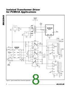
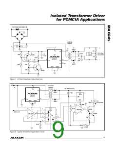
Figure 3. 5V to Isolated 5V Application Circuit
Figure 4. 3.3V Input to Isolated Output Application Circuit
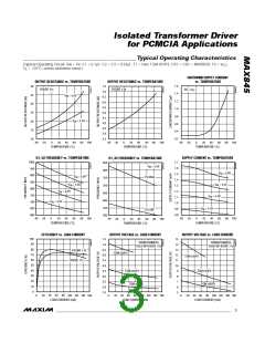
The MAX845 is a versatile transformer driver, capable
of driving a center-tapped transformer primary from a
5V or 3.3V DC power supply (Figures 3 and 4). The
secondary can be wound to provide any isolated volt-
age needed at power levels up to 750mW with a 5V
supply or up to 500mW with a 3.3V supply. Figure 3
shows a typical 5V to isolated 5V application circuit that
delivers up to 150mA of isolated 5V power.
will be higher at 3.3V, so transformer winding resistance
will be more critical and efficiencies will be lower. The
MAX845 output current must still be limited to 200mA
(see Absolute Maximum Ratings), so the available out-
put power will be less than with a 5V power source.
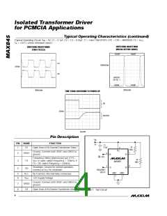
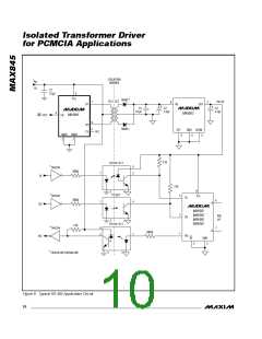
Lo w -No is e P o w e r S u p p ly
The MAX845 topology is inherently low noise, in that
either one or the other of the two power devices is on at
any given time. By alternating between two identical
states with one side on and the other off, the input cur-
rent is nearly constant and secondary output power is
available at all times. There is an intentional break-
before-make action to prevent any possibility of both
power switches conducting at the same time. During
this 100ns non-overlap interval, the input current goes
to zero. This adds a small high-frequency component
to the input current waveform. This ripple current can
easily be absorbed by a small input bypass capacitor
3 .3 V S u p p ly
Any of the application circuits shown may be converted
to 3.3V operation by changing the turns ratio of the trans-
former and operating the MAX845 from a boost supply,
as shown in Figure 4. In normal operation, whenever one
of the MAX845 outputs goes low, the other goes to
approximately double the supply voltage. Since the cir-
cuit is symmetrical, the two outputs can be combined
with diodes, lightly filtered, then used to power the
MAX845, and possibly other light loads as well.
(0.33µF) from V
noise bias supply using the MAX845 transformer driver.
to ground. Figure 5 shows a low-
CC
The diodes on the primary side may be any fast-switch-
ing small-signal diodes, such as the 1N914, 1N4148, or
CMPD2838. The value of the primary filter capacitor is
not critical and can be very small, since it only needs to
supply current to the MAX845 during the break-before-
make interval.
Whe n us ing the two-d iod e p us h-p ull (Fig ure 11a )
rectifier or the four-diode bridge (Figure 11b), the out-
put voltage tends to be more constant than in most
alternative topologies. As described above, the circuit
alternates between two identical states that both pro-
vide power to the load. The only part of the cycle that
produces output ripple is the 100ns non-overlap inter-
val, which can easily be filtered by a small ceramic
output capacitor (0.33µF).
The transformer could be any of the same ones used for
5V operation, but for optimum performance it should
have fewer primary turns, as the ET product required is
now only 3.3V-µs. For a given power level, the currents
6
_______________________________________________________________________________________

 MAXIM [ MAXIM INTEGRATED PRODUCTS ]