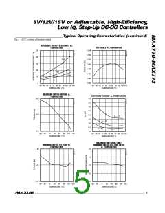
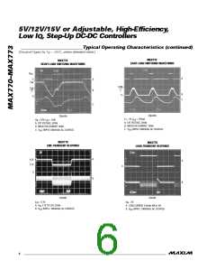
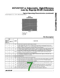
5 V/1 2 V/1 5 V o r Ad ju s t a b le , High-Effic ie nc y,
Low I , Ste p-Up DC-DC Controlle rs
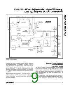
Q
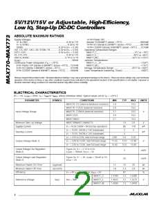
ABSOLUTE MAXIMUM RATINGS
Supply Voltages
14-Pin Plastic DIP
V+ to GND.............................................................-0.3V to 17V
V+ to SGND.............................................................-0.3V to 7V
SGND........................................................-0.3V to (V+ + 0.3V)
EXT, CS, REF, LBO, LBI, SHDN, FB.............-0.3V to (V+ + 0.3V)
EXTH, EXTL ..................................................-0.3V to (V+ + 0.3V)
V5, V12, V15 .............................................................-0.3V to 17V
GND to AGND .........................................................0.1V to -0.1V
(derate 10.00mW/°C above +70°C) .............................800mW
14-Pin SO (derate 8.33mW/°C above +70°C) ..............667mW
14-Pin CERDIP (derate 9.09mW/°C above +70°C)......727mW
Operating Temperature Ranges
MAX77_C__ ........................................................0°C to +70°C
MAX77_E__......................................................-40°C to +85°C
MAX77_MJ_ ...................................................-55°C to +125°C
Junction Temperatures
I
..................................................................................50mA
SGND
Continuous Power Dissipation (T = +70°C)
MAX77_C__/E__ ..........................................................+150°C
MAX77_MJ_..................................................................+175°C
Storage Temperature Range .............................-65°C to +160°C
Lead Temperature (soldering, 10sec).............................+300°C
A
8-Pin Plastic DIP (derate 9.09mW/°C above +70°C)....727mW
8-Pin SO (derate 5.88mW/°C above +70°C) ................471mW
8-Pin CERDIP (derate 8.00mW/°C above +70°C) ........640mW
Stresses beyond those listed under “Absolute Maximum Ratings” may cause permanent damage to the device. These are stress ratings only, and functional
operation of the device at these or any other conditions beyond those indicated in the operational sections of the specifications is not implied. Exposure to
absolute maximum rating conditions for extended periods may affect device reliability.
0–MAX73
ELECTRICAL CHARACTERISTICS
(V+ = 5V, I
= 0mA, T = T
to T , unless otherwise noted. Typical values are at T = +25°C.)
MAX A
LOAD
A
MIN
PARAMETER
SYMBOL
CONDITIONS
MIN
2.0
3.0
3.1
3.0
3.1
TYP
MAX
16.5
16.5
16.5
16.5
16.5
2.0
UNITS
MAX770–772 (internal feedback resistors)
MAX770–772C/E (external resistors)
MAX770–772MJA (external resistors)
MAX773C/E
Input Voltage Range
V
MAX773MJD
Minimum Start-Up Voltage
Supply Current
MAX770/MAX771/MAX772
1.8
85
V
µA
V+ = 16.5V, SHDN = 0V (normal operation)
V+ = 10.0V, SHDN ≥ 1.6V (shutdown)
V+ = 16.5V, SHDN ≥ 1.6V (shutdown)
V+ = 2.0V to 5.0V, over full load range
V+ = 2.0V to 12.0V, over full load range
V+ = 2.0V to 15.0V, over full load range
110
5
2
µA
Standby Current
4
4.80
11.52
14.40
5.0
12.0
15.0
5.20
12.48
15.60
Output Voltage (Note 1)
V
Output Voltage Line Regulation
(Note 2)
Figure 2a, V+ = 2.7V to 4.5V,
5
mV/V
mV/A
I
= 700mA, V
= 5V
LOAD
OUT
Output Voltage Load Regulation
(Note 2)
Figure 2a, V+ = 3V, I
= 30mA to 1A,
LOAD
20
V
OUT
= 5V
µs
µs
%
Maximum Switch On-Time
Minimum Switch Off-Time
Efficiency
t
(max)
12
16
2.3
87
20
ON
t
(min)
1.8
2.8
OFF
V+ = 4V, I
= 500mA, V
= 5V
LOAD
OUT
MAX77_C
MAX77_E
MAX77_M
1.4700
1.4625
1.4550
1.5
1.5
1.5
1.5300
1.5375
1.5450
I
0µA
Reference Voltage
V
REF
V
REF =
_______________________________________________________________________________________
2

 MAXIM [ MAXIM INTEGRATED PRODUCTS ]