Cold-Junction-Compensated K-Thermocouple-
to-Digital Converter (0°C to +1024°C)
ABSOLUTE MAXIMUM RATINGS
Supply Voltage (V
to GND) ................................ -0.3V to +6V
Storage Temperature Range ............................-65°C to +150°C
Junction Temperature .................................................... +150°C
SO Package
CC
SO, SCK, CS, T-, T+ to GND .......................-0.3V to V
SO Current ........................................................................ 50mA
+ 0.3V
CC
ESD Protection (Human Body Model) ........................... 2000V
Vapor Phase (60s) . .....................................................+215°C
Infrared (15s) ..............................................................+220°C
Lead Temperature (soldering, 10s) ............................... +300°C
Continuous Power Dissipation (T = +70°C)
A
8-Pin SO (derate 5.88mW/°C above +70°C) .............. 471mW
Operating Temperature Range ..........................-20°C to +85°C
Stresses beyond those listed under “Absolute Maximum Ratings” may cause permanent damage to the device. These are stress ratings only, and functional
operation of the device at these or any other conditions beyond those indicated in the operational sections of the specifications is not implied. Exposure to
absolute maximum rating conditions for extended periods may affect device reliability.
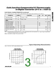
ELECTRICAL CHARACTERISTICS
(V
= +3.0V to +5.5V, T = -20°C to +85°C, unless otherwise noted. Typical values specified at +25°C.) (Note 1)
A
CC
PARAMETER
SYMBOL
CONDITIONS
MIN
-5
TYP
MAX
+5
UNITS
V
V
V
V
= +3.3V
= +5V
CC
CC
CC
CC
T
= +700°C,
THERMOCOUPLE
T = +25°C (Note 2)
A
-6
+6
= +3.3V
= +5V
-8
+8
T
= 0°C to
THERMOCOUPLE
+700°C, T = +25°C (Note 2)
A
-9
+9
Temperature Error
LSB
T
= +700 C
V
V
= +3.3V
= +5V
-17
-19
+17
+19
THERMOCOUPLE
CC
CC
to +1000 C, T = +25 C
A
(Note 2)
Thermocouple Conversion
Constant
10.25
µV/LSB
V
V
= +3.3V
= +5V
-3.0
-3.0
+3.0
+3.0
CC
CC
Cold-Junction
Compensation Error
T = -20°C to +85°C
A
(Note 2)
°C
°C
k
Resolution
0.25
60
Thermocouple Input
Impedance
Supply Voltage
V
3.0
1
5.5
1.5
2.5
V
mA
V
CC
Supply Current
I
0.7
2
CC
Power-On Reset Threshold
Power-On Reset Hysteresis
Conversion Time
V
rising
CC
50
mV
s
(Note 2)
0.17
0.22
SERIAL INTERFACE
0.3 x
Input Low Voltage
Input High Voltage
V
V
V
IL
V
CC
0.7 x
V
IH
V
CC
Input Leakage Current
Input Capacitance
I
V
= GND or V
CC
5
µA
pF
LEAK
IN
C
5
IN
2
_______________________________________________________________________________________

 MAXIM [ MAXIM INTEGRATED PRODUCTS ]