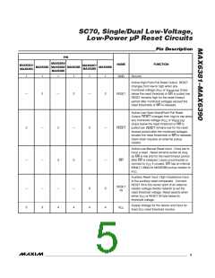
SC70, Single/Dual Low-Voltage,
Low-Power µP Reset Circuits
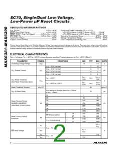
ABSOLUTE MAXIMUM RATINGS
CC
V
to GND..........................................................-0.3V to +6.0V
Continuous Power Dissipation (T = +70°C)
A
RESET Open-Drain Output....................................-0.3V to +6.0V
3-Pin SC70 (derate 2.9mW/°C above +70°C)........235mW
4-Pin SC70 (derate 3.1mW/°C above +70°C)........245mW
Operating Temperature Range .........................-40°C to +125°C
Storage Temperature Range.............................-65°C to +150°C
Lead Temperature (soldering, 10s) .................................+300°C
RESET, RESET (Push-Pull Output) .............-0.3V to (V
MR, RESET IN.............................................-0.3V to (V
+ 0.3V)
+ 0.3V)
CC
CC
Input Current (V ).............................................................20mA
CC
Output Current (All Pins).....................................................20mA
Stresses beyond those listed under “Absolute Maximum Ratings” may cause permanent damage to the device. These are stress ratings only, and functional
operation of the device at these or any other conditions beyond those indicated in the operational sections of the specifications is not implied. Exposure to
absolute maximum rating conditions for extended periods may affect device reliability.
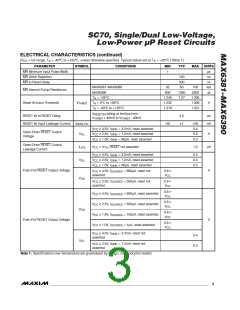
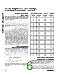
ELECTRICAL CHARACTERISTICS
(V
= full range, T = -40°C to +125°C, unless otherwise specified. Typical values are at T = +25°C.) (Note 1)
CC
A
A
PARAMETER
SYMBOL
CONDITIONS
MIN
TYP
MAX
5.5
13
11
7
UNITS
Operating Voltage Range
V
1.0
V
CC
V
V
V
V
= 5.5V, no load
7
6
4
3
CC
CC
CC
CC
= 3.6V, no load
= 2.5V, no load
= 1.8V, no load
V
Supply Current
I
µA
V
CC
CC
6
V
-
V
+
TH
TH
T
T
= +25°C
V
V
A
A
TH
TH
1.5%
1.5%
V
Reset Threshold
CC
V
TH
(See Reset Thresholds table)
Reset Threshold Tempco
V
-
V
+
TH
TH
= -40°C to +125°C
2.5%
2.5%
∆V /°C
60
35
ppm/°C
TH
V
falling at 10mV/µs from V + 100mV
TH
CC
V
to Reset Delay
µs
CC
to V - 100mV
TH
D1
D2
D3
D5
D6
D4
D7
1
2
20
40
140
280
560
1120
1200
140
150
1120
1200
280
Reset Timeout Period
MAX6381–MAX6389
(See Reset Timeout table)
t
ms
560
RP
1120
2240
2400
280
D4
D7
D4
D7
MR timeout period
300
Reset Timeout Period
MAX6390
t
RP
ms
2240
2400
V
V
V
timeout period
< 4V
CC
TH
TH
✕
0.3
CC
V
V
IL
V
✕
0.7
MR Input Voltage
V
IH
V
CC
V
0.8
IL
> 4V
V
2.4
IH
2
_______________________________________________________________________________________

 MAXIM [ MAXIM INTEGRATED PRODUCTS ]