Ultra-Low Offset/Drift, Low-Noise,
Precision SOT23 Amplifiers
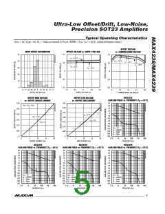
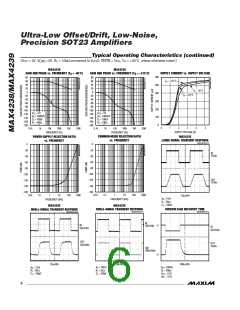
Typical Operating Characteristics (continued)
(V
= 5V, V
= 0V, R = 10kΩ connected to V /2, SHDN = V , T = +25°C, unless otherwise noted.)
CC
L
CC
CC
A
CM
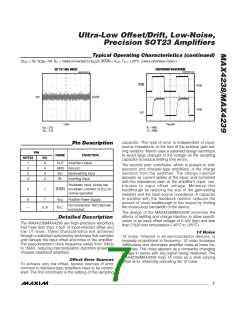
SHUTDOWN WAVEFORM
DC TO 10Hz NOISE
MAX4238/39 toc20
MAX4238/39 toc19
SHDN
2V/div
1V/div
2µV/div
OUT
OUT
10µs/div
1s/div
R = 10kΩ
L
V
V
= 2.5V
= -2.5V
L
CC
EE
C = 100pF
capacitor. This type of error is independent of input-
source impedance, or the size of the external gain-set-
ting resistors. Maxim uses a patented design technique
to avoid large changes in the voltage on the sampling
capacitor to reduce settling time errors.
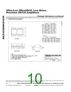
Pin Description
PIN
NAME
FUNCTION
SOT23
SO
6
1
2
3
4
OUT
Amplifier Output
The second error contributor, which is present in both
autozero and chopper-type amplifiers, is the charge
injection from the switches. The charge injection
appears as current spikes at the input, and combined
with the impedance seen at the amplifier’s input, con-
tributes to input offset voltage. Minimize this
feedthrough by reducing the size of the gain-setting
resistors and the input-source impedance. A capacitor
in parallel with the feedback resistor reduces the
amount of clock feedthrough to the output by limiting
the closed-loop bandwidth of the device.
4
GND Ground
3
IN+
IN-
Noninverting Input
2
Inverting Input
Shutdown Input. Active low
shutdown, connect to V
normal operation.
for
5
1
SHDN
CC
6
7
V
Positive Power Supply
CC
No Connection. Not internally
connected.
—
5, 8
N.C.
The design of the MAX4238/MAX4239 minimizes the
effects of settling and charge injection to allow specifi-
cation of an input offset voltage of 0.1µV (typ) and less
than 2.5µV over temperature (-40°C to +85°C).
Detailed Description
The MAX4238/MAX4239 are high-precision amplifiers
that have less than 2.5µV of input-referred offset and
low 1/f noise. These characteristics are achieved
through a patented autozeroing technique that samples
and cancels the input offset and noise of the amplifier.
The pseudorandom clock frequency varies from 10kHz
to 15kHz, reducing intermodulation distortion present in
chopper-stabilized amplifiers.
1/f Noise
1/f noise, inherent in all semiconductor devices, is
inversely proportional to frequency. 1/f noise increases
3dB/octave and dominates amplifier noise at lower fre-
quencies. This noise appears as a constantly changing
voltage in series with any signal being measured. The
MAX4238/MAX4239 treat 1/f noise as a slow varying
offset error, inherently canceling the 1/f noise.
Offset Error Sources
To achieve very low offset, several sources of error
common to autozero-type amplifiers need to be consid-
ered. The first contributor is the settling of the sampling
_______________________________________________________________________________________
7

 MAXIM [ MAXIM INTEGRATED PRODUCTS ]