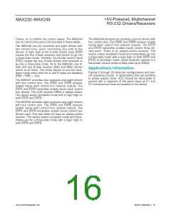
+5V-Powered, Multichannel
RS-232 Drivers/Receivers
MAX220–MAX249
mode% in three-state mode% or when device power is
removedꢂ Outputs can be driven to ±±5Vꢂ ꢅhe power-
supply current typically drops to 8ꢃM in shutdown modeꢂ
ꢅhe ꢄMAXX1 does not have pullup resistors to force the
outputs of the unused drivers lowꢂ Connect unused
Detailed Description
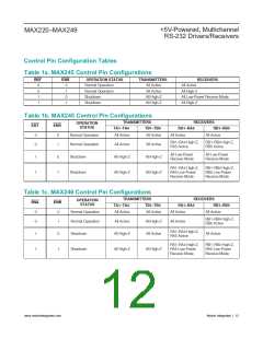
ꢅhe ꢄMAXX1ꢀꢄMAXꢁ9 contain four sections: dual
charge-pump DC-DC voltage converters% RS-X.X dri-
vers% RS-X.X receivers% and receiver and transmitter
enable control inputsꢂ
inputs to GND or V
ꢂ
CC
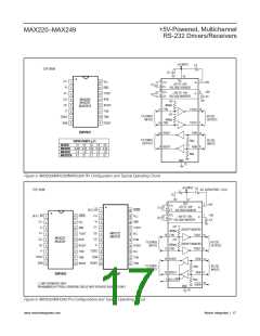
Dual Charge-Pump Voltage Converter
ꢅhe ꢄMAXX1ꢀꢄMAXꢁ9 have two internal charge-pumps
that convert +5V to ±±1V (unloaded) for RS-X.X driver
operationꢂ ꢅhe first converter uses capacitor C± to dou-
ble the +5V input to +±1V on C. at the V+ outputꢂ ꢅhe
second converter uses capacitor CX to invert +±1V to
-±1V on Cꢁ at the V- outputꢂ
ꢅhe ꢄMAX.9 has a receiver three-state control line% and
the ꢄMAXX.% ꢄMAXX5% ꢄMAX.5% ꢄMAX.6% ꢄMAXꢁ1%
and ꢄMAXꢁ± have both a receiver three-state control
line and a low-power shutdown controlꢂ ꢅable X shows
the effects of the shutdown control and receiver three-
state control on the receiver outputsꢂ
ꢅhe receiver ꢅꢅL/CꢄOS outputs are in a high-imped-
ance% three-state mode whenever the three-state enable
line is high (for the ꢄMAXX5/ꢄMAX.5/ꢄMAX.6/ꢄMAX.9ꢀ
ꢄMAXꢁ±)% and are also high-impedance whenever the
shutdown control line is highꢂ
M small amount of power may be drawn from the +±1V
(V+) and -±1V (V-) outputs to power external circuitry
(see the ꢅypical Operating Characteristics section)%
except on the ꢄMAXX5 and ꢄMAXꢁ5ꢀꢄMAXꢁ4% where
these pins are not availableꢂ V+ and V- are not regulated%
so the output voltage drops with increasing load currentꢂ
Do not load V+ and V- to a point that violates the mini-
mum ±5V EIM/ꢅIM-X.XE driver output voltage when
sourcing current from V+ and V- to external circuitryꢂ
When in low-power shutdown mode% the driver outputs
are turned off and their leakage current is less than ±ꢃM
with the driver output pulled to groundꢂ ꢅhe driver output
leakage remains less than ±ꢃM% even if the transmitter
output is backdriven between 1V and (V
+ 6V)ꢂ Below
CC
-1ꢂ5V% the transmitter is diode clamped to ground with
When using the shutdown feature in the ꢄMAXXX%
ꢄMAXX5% ꢄMAX.1% ꢄMAX.5% ꢄMAX.6% ꢄMAXꢁ1%
ꢄMAXꢁ±% and ꢄMAXꢁ5ꢀꢄMAXꢁ9% avoid using V+ and V-
to power external circuitryꢂ When these parts are shut
down% V- falls to 1V% and V+ falls to +5Vꢂ µor applica-
tions where a +±1V external supply is applied to the V+
pin (instead of using the internal charge pump to gen-
erate +±1V)% the C± capacitor must not be installed and
±kΩ series impedanceꢂ ꢅhe transmitter is also zener
clamped to approximately V
impedance of ±kΩꢂ
+ 6V% with a series
CC
ꢅhe driver output slew rate is limited to less than .1V/ꢃs
as required by the EIM/ꢅIM-X.XE and VꢂX8 specifica-
tionsꢂ ꢅypical slew rates are XꢁV/ꢃs unloaded and
±1V/ꢃs loaded with .Ω and X511pµꢂ
the SHDN pin must be connected to V ꢂ ꢅhis is
CC
because V+ is internally connected to V
modeꢂ
in shutdown
RS-232 Receivers
CC
EIM/ꢅIM-X.XE and VꢂX8 specifications define a voltage
level greater than .V as a logic 1% so all receivers invertꢂ
Input thresholds are set at 1ꢂ8V and XꢂꢁV% so receivers
respond to ꢅꢅL level inputs as well as EIM/ꢅIM-X.XE and
VꢂX8 levelsꢂ
RS-232 Drivers
ꢅhe typical driver output voltage swing is ±8V when
loaded with a nominal 5kΩ RS-X.X receiver and V
=
CC
+5Vꢂ Output swing is guaranteed to meet the EIM/ꢅIM-
X.XE and VꢂX8 specification% which calls for ±5V mini-
mum driver output levels under worst-case conditionsꢂ
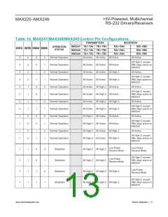
Table 2. Three-State Control of
Receivers
ꢅhese include a minimum .kΩ load% V
= +ꢁꢂ5V% and
CC
maximum operating temperatureꢂ Unloaded driver out-
put voltage ranges from (V+ -±ꢂ.V) to (V- +1ꢂ5V)ꢂ
PART
SHDN
EN
EN(R)
RECEIVERS
SHDN
Input thresholds are both ꢅꢅL and CꢄOS compatibleꢂ
ꢅhe inputs of unused drivers can be left unconnected
Low
High Low
High High
A
High Impedance
Mctive
High Impedance
ꢄMAXX.
__
__
since ꢁ11kΩ input pullup resistors to V
are built in
CC
(except for the ꢄMAXX1)ꢂ ꢅhe pullup resistors force the
outputs of unused drivers low because all drivers invertꢂ
ꢅhe internal input pullup resistors typically source ±XꢃM%
except in shutdown mode where the pullups are dis-
abledꢂ Driver outputs turn off and enter a high-imped-
ance state—where leakage current is typically
microamperes (maximum X5ꢃM)—when in shutdown
Low
High
High Impedance
Mctive
ꢄMAXX5
__
__
__
__
__
ꢄMAX.5 Low
ꢄMAX.6 Low
ꢄMAXꢁ1 High
Low
High
A
High Impedance
Mctive
High Impedance
www.maximintegrated.com
Maxim Integrated | 14

 MAXIM [ MAXIM INTEGRATED PRODUCTS ]