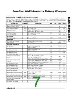
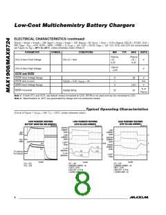
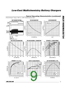
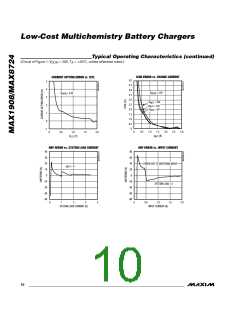
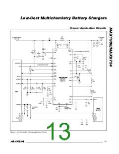
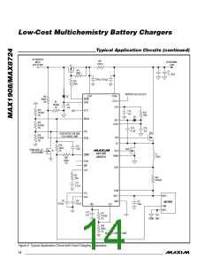
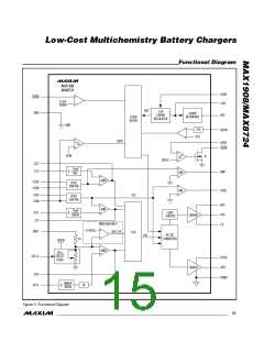
Low-Cost Multichemistry Battery Chargers
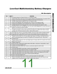
Pin Description
PIN
1
NAME
DCIN
LDO
CLS
FUNCTION
Charging Voltage Input. Bypass DCIN with a 1µF capacitor to PGND.
2
Device Power Supply. Output of the 5.4V linear regulator supplied from DCIN. Bypass with a 1µF capacitor to GND.
Source Current-Limit Input. Voltage input for setting the current limit of the input source.
4.096V Voltage Reference. Bypass REF with a 1µF capacitor to GND.
3
4
REF
5
CCS
CCI
Input-Current Regulation Loop-Compensation Point. Connect a 0.01µF capacitor to GND.
Output-Current Regulation Loop-Compensation Point. Connect a 0.01µF capacitor to GND.
Voltage Regulation Loop-Compensation Point. Connect 1kΩ in series with 0.1µF capacitor to GND.
6
7
CCV
Shutdown Control Input. Drive SHDN logic low to shut down the MAX1908/MAX8724. Use with a thermistor to
detect a hot battery and suspend charging.
8
9
SHDN
Charge-Current Monitor Output. ICHG is a scaled-down replica of the charger output current. Use ICHG to
monitor the charging current and detect when the chip changes from constant-current mode to constant-
voltage mode. The transconductance of (CSIP - CSIN) to ICHG is 3µA/mV.
ICHG
ACIN
10
11
12
AC Detect Input. Input to an uncommitted comparator. ACIN can be used to detect AC-adapter presence.
ACOK AC Detect Output. High-voltage open-drain output is high impedance when V
is less than V
/ 2.
REF
ACIN
REFIN Reference Input. Allows the ICTL and VCTL inputs to have ratiometric ranges for increased accuracy.
Output Current-Limit Set Input. ICTL input voltage range is V
/ 32 to V
. The device shuts down if
REFIN
REFIN
13
14
15
ICTL
GND
VCTL
BATT
ICTL is forced below V
/ 100. When ICTL is equal to LDO, the set point for CSIP - CSIN is 45mV.
REFIN
Analog Ground
Output-Voltage Limit Set Input. VCTL input voltage range is 0 to V
point is (4.2 x CELLS) V.
. When VCTL is equal to LDO, the set
REFIN
16
17
18
19
20
21
22
23
24
25
26
27
Battery Voltage Input
CELLS Cell Count Input. Trilevel input for setting number of cells. GND = 2 cells, float = 3 cells, REFIN = 4 cells.
CSIN
CSIP
Output Current-Sense Negative Input
Output Current-Sense Positive Input. Connect a current-sense resistor from CSIP to CSIN.
PGND Power Ground
DLO
DLOV
LX
Low-Side Power MOSFET Driver Output. Connect to low-side NMOS gate.
Low-Side Driver Supply. Bypass DLOV with a 1µF capacitor to GND.
High-Side Power MOSFET Driver Power-Return Connection. Connect to the source of the high-side NMOS.
High-Side Power MOSFET Driver Power-Supply Connection. Connect a 0.1µF capacitor from LX to BST.
High-Side Power MOSFET Driver Output. Connect to high-side NMOS gate.
Input Current-Sense Negative Input
BST
DHI
CSSN
CSSP
Input Current-Sense Positive Input. Connect a current-sense resistor from CSSP to CSSN.
Input-Current Monitor Output. IINP is a scaled-down replica of the input current. IINP monitors the total
system current. The transconductance of (CSSP - CSSN) to IINP is 3µA/mV.
28
IINP
______________________________________________________________________________________ 11

 MAXIM [ MAXIM INTEGRATED PRODUCTS ]