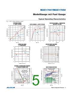
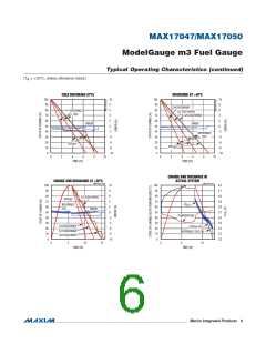
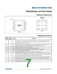
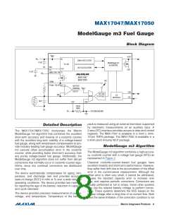
MAX17047/MAX17050
ModelGauge m3 Fuel Gauge
ELECTRICAL CHARACTERISTICS (2-WIRE INTERFACE) (continued)
(2.5V P V
P 4.5V, T = -20NC to +70NC.) (Note 1)
A
BATT
PARAMETER
SYMBOL
CONDITIONS
MIN
TYP
MAX
UNITS
ns
Fall Time of Both SDA and SCL
Signals
20 +
t
300
F
0.1C
B
Setup Time for STOP Condition
t
0.6
Fs
SU:STO
Spike Pulse Widths
Suppressed by Input Filter
t
(Note 7)
(Note 8)
0
50
ns
SP
Capacitive Load for Each Bus
Line
C
400
60
pF
pF
B
SCL, SDA Input Capacitance
C
BIN
Note 1: Specifications are 100% tested at T = +25°C. Limits over the operating range are guaranteed by design and
A
characterization.
Note 2: All voltages are referenced to CSP.
Note 3: Timing must be fast enough to prevent the device from entering shutdown mode due to bus low for a period > 45s minimum.
Note 4: f
must meet the minimum clock low time plus the rise/fall times.
SCL
Note 5: The maximum t
has only to be met if the device does not stretch the low period (t
) of the SCL signal.
HD:DAT
LOW
Note 6: This device internally provides a hold time of at least 100ns for the SDA signal (referred to the minimum VIH of the SCL
signal) to bridge the undefined region of the falling edge of SCL.
Note 7: Filters on SDA and SCL suppress noise spikes at the input buffers and delay the sampling instant.
Note 8: C —total capacitance of one bus line in pF.
B
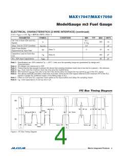
2
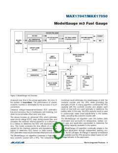
I C Bus Timing Diagram
SDA
t
F
t
SP
t
t
BUF
t
R
F
t
SU:DAT
t
t
t
R
HD:STA
LOW
SCL
t
t
t
SU:STO
HD:STA
SU:STA
t
HD:DAT
P
S
Sr
S
2
Figure 1. I C Bus Timing Diagram
����������������������������������������������������������������� Maxim Integrated Products
4

 MAXIM [ MAXIM INTEGRATED PRODUCTS ]