Mu lt i-Ou t p u t , Lo w -No is e P o w e r-S u p p ly
Co n t ro lle rs fo r No t e b o o k Co m p u t e rs
0–MAX1635
where t is the diode-conduction time (120ns typical)
Re c tifie r d iod e c a thod e to low-s id e
MOSFET: 5mm max length
D
and V
is the forward voltage of the diode.
FWD
LX nod e (MOSFETs , re c tifie r c a thod e ,
inductor): 15mm max length
This power is dissipated in the MOSFET body diode if
no external Schottky diode is used.
Ideally, surface-mount power components are butted
up to one another with their ground terminals almost
touching. These high-current grounds are then con-
nected to each other with a wide filled zone of top-layer
copper so they don’t go through vias. The resulting top-
layer “sub-ground-plane” is connected to the normal
inner-layer ground plane at the output ground termi-
nals, which ensures that the IC’s analog ground is
sensing at the supply’s output terminals without interfer-
ence from IR drops and ground noise. Other high-
current paths should also be minimized, but focusing
primarily on short ground and current-sense con-
nections eliminates about 90% of all PC board lay-
out problems (s e e the PC b oa rd la youts in the
MAX1630 Evaluation Kit manual for examples).
2
P(cap) = input capacitor ESR loss = (I
)
x R
ESR
RMS
where I
is the input ripple current as calculated in the
Design Procedure and Input Capacitor Value sections.
RMS
Lig h t -Lo a d Effic ie n c y Co n s id e ra t io n s
Under light loads, the PWM operates in discontinuous
mode, where the inductor current discharges to zero at
some point during the switching cycle. This makes the
inductor current’s AC component high compared to the
load current, which increases core losses and I2R loss-
es in the output filter capacitors. For best light-load effi-
c ie nc y, us e MOSFETs with mod e ra te g a te -c ha rg e
levels, and use ferrite, MPP, or other low-loss core
material. Avoid powdered-iron cores; even Kool-Mu
(aluminum alloy) is not as good as ferrite.
2) Place the IC and signal components. Keep the main
switching nodes (LX nodes) away from sensitive
analog components (current-sense traces and REF
capacitor). Place the IC and analog components on
the op p os ite s id e of the b oa rd from the p owe r-
switching node. Important: the IC must be no far-
ther than 10mm from the current-sense resistors.
Keep the gate-drive traces (DH_, DL_, and BST_)
shorter than 20mm and route them away from CSH_,
CSL_, and REF.
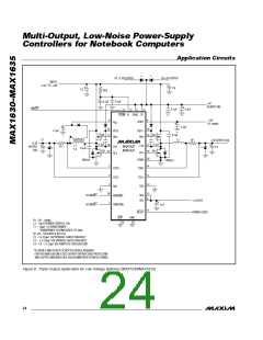
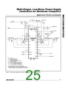
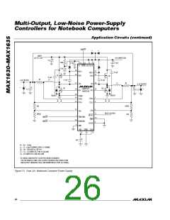
P C Bo a rd La yo u t Co n s id e ra t io n s
Good PC board layout is required in order to achieve
specified noise, efficiency, and stability performance.
The PC b oa rd la yout a rtis t mus t b e g ive n e xp lic it
instructions, preferably a pencil sketch showing the
placement of power-switching components and high-
c urre nt routing . Se e the PC b oa rd la yout in the
MAX1630 Eva lua tion Kit ma nua l for e xa mp le s . A
ground plane is essential for optimum performance. In
most applications, the circuit will be located on a multi-
layer board, and full use of the four or more copper lay-
ers is recommended. Use the top layer for high-current
connections, the bottom layer for quiet connections
(REF, SS, GND), and the inner layers for an uninterrupt-
ed ground plane. Use the following step-by-step guide:
3) Us e a s ing le -p oint s ta r g round whe re the inp ut
ground trace, power ground (sub-ground-plane),
and normal ground plane meet at the supply’s out-
put ground terminal. Connect both IC ground pins
and all IC bypass capacitors to the normal ground
plane.
1) Place the high-power components (Figure1, C1, C3,
Q1, Q2, D1, L1, and R1) first, with any grounded
connections adjacent.
HIGH CURRENT PATH
Priority 1: Minimize current-sense resistor trace
lengths a nd e ns ure a c c ura te c urre nt
sensing with Kelvin connections (Figure 7).
SENSE RESISTOR
Priority 2: Minimize ground trace lengths in the
high-current paths (discussed below).
Priority 3: Minimize other trace lengths in the high-
current paths.
Use >5mm-wide traces
C
to high-side MOSFET drain: 10mm
MAX1630
IN
max length
Figure 7. Kelvin Connections for the Current-Sense Resistors
______________________________________________________________________________________ 23

 MAXIM [ MAXIM INTEGRATED PRODUCTS ]