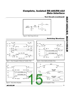
Complete, Isolated RS-485/RS-422
Data Interface
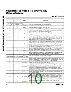
___________________________________________________Pin Description (continued)
PIN
NAME
FUNCTION
MAX1480A/B/C MAX1490A/B
PINS ON THE ISOLATED RS-485/RS-422 SIDE (continued)
—
—
—
—
21
22
23
17
18
19
20
—
—
—
Y
Noninverting Driver Output
Inverting Driver Output
Inverting Receiver Input
Noninverting Receiver Input
Isolated Driver-Enable Input. Connect to ISO DE DRV for normal operation.
Isolated Driver Input. Connect to ISO DI DRV for normal operation.
Noninverting Driver Output and Noninverting Receiver Input
Z
B
A
ISO DE IN
ISO DI IN
A
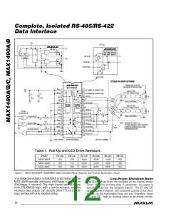
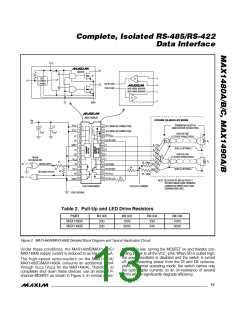
Isolated Receiver-Output Drive. Connect to ISO RO LED through a resistor
(Table 1 of Figure 1 for MAX1480A/B/C, Table 2 of Figure 2 for MAX1490A/B).
24
21
ISO RO DRV
25
26
—
22
B
Inverting Driver Output and Inverting Receiver Input
Isolated Supply Voltage Source
ISO V
CC1
27, 28
23, 24
AC2, AC1
Internal Connections. Leave these pins unconnected.
Note: For DE´ and DI´ pin descriptions, see Detailed Block Diagram and Typical Application Circuit (Figure 1 for MAX1480A/B/C,
Figure 2 for MAX1490A/B).
Use the FS pin to select between high and low switching
Detailed Description
frequencies for the isolated power driver. The driver
The MAX1480A/MAX1480B/MAX1480C/MAX1490A/
switches at the lower frequency 535kHz when FS is low,
MAX1490B are complete, electrically isolated, RS-485/
and at the higher frequency 725kHz when FS is high. The
RS-422 data-communications interface solutions.
FS pin has a weak internal pull-up that switches the
Transceivers, optocouplers, a power driver, and a
device to the high-frequency mode when FS is left
transformer in one standard 28-pin DIP package (24-
unconnected. With FS high or open, no-load supply
pin for the MAX1490A/B) provide a complete interface.
current is reduced by approximately 4mA, and by up to
Signals and power are internally transported across the
8mA when fully loaded. For optimal performance and
isolation barrier (Figures 1, 2). Power is transferred from
minimal supply current, connect FS to V
unconnected.
or leave
CC_
the logic side (nonisolated side) to the isolated side of
the barrier through a center-tapped transformer.
Signals cross the barrier through high-speed optocou-
plers. A single +5V supply on the logic side powers
both sides of the interface. The MAX1480A/B/C offer
half-duplex communications while the MAX1490A/B
feature full-duplex communication. The functional
input/output relationships are shown in Tables 3–6.
Drivers are short-circuit current limited and are protect-
ed against excessive power dissipation by thermal
shutdown circuitry that puts the driver outputs into a
high-impedance state. The receiver input has a fail-safe
feature that guarantees a logic-high RO (logic-low RO)
output if the input is open circuit.
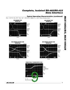
On the MAX1480A/B/C, the driver outputs are enabled
by bringing DE´ high. Driver-enable times are typically
0.2µs for the MAX1480A, 35µs for the MAX1480B, and
0.5µs for the MAX1480C. Allow time for the devices to be
enabled before sending data (see the Driver Enable
Time vs. Temperature graph in the Typical Operating
Characteristics). When enabled, driver outputs function
as line drivers. Driver outputs are high impedance when
DE´ is low. While outputs are high impedance, they func-
tion as line receivers.
The MAX1480B/MAX1480C/MAX1490B feature reduced-
slew-rate drivers that minimize EMI and reduce reflec-
tions caused by improperly terminated cables, allowing
error-free transmission at data rates up to 250kbps. The
MAX1480A/MAX1490A driver slew rate is not limited,
allowing transmission rates up to 2.5Mbps.
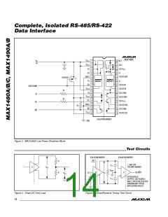
The MAX1480B/MAX1480C/MAX1490B shutdown feature
reduces supply current to as low as 0.2µA by using the
SD pin (see Low-Power Shutdown Mode section).
______________________________________________________________________________________ 11

 MAXIM [ MAXIM INTEGRATED PRODUCTS ]