Complete, Isolated RS-485/RS-422
Data Interface
________________________________________________________________Pin Description
PIN
NAME
FUNCTION
MAX1480A/B/C MAX1490A/B
PPININSSOONNTTHHEENNOONN-I-SISOOLLAATTEEDDSSIDIDEE
1, 2, 8, 10
1, 2, 8, 10
V
–V
Logic-Side (nonisolated side) +5V Supply Voltages
Internal Connections. Leave these pins unconnected.
Logic-Side Ground. Connect to GND2 (pin 12).
CC1 CC4
3, 4
5
3, 4
5
D1, D2
GND1
Frequency Select Input. If FS = V
or is open, switch frequency is high; if FS
CC_
6
7
6
7
FS
= GND, switch frequency is low. For optimal performance and minimal supply
current, connect FS to V or leave unconnected.
CC_
Shutdown Input. Ground for normal operation. When high, the power oscillator is
disabled.
SD
Driver Input. With DE´ high (MAX1480A/B/C only), a low on DI´ forces output A
low and output B high. Similarly, a high on DI´ forces output A high and output
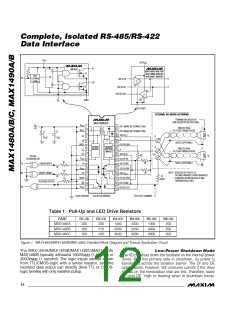
B low. Drives internal LED cathode through a resistor (Table 1 of Figure 1 for
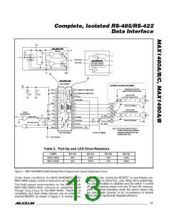
MAX1480A/B/C, Table 2 of Figure 2 for MAX1490A/B).
9
9
DI
Driver-Enable Input. The driver outputs, A and B, are enabled by bringing DE´
high. The driver outputs are high impedance when DE´ is low. If the driver out-
puts are enabled, the device functions as a line driver. While the driver outputs
are high impedance, the device functions as a line receiver. Drives internal
LED cathode through a resistor (Table 1 of Figure 1).
11
—
DE
Receiver Output. If A > B by 200mV, RO will be high; if A < B by 200mV, RO
—
12
13
14
11
12
—
—
RO
GND2
RO
will be low. Open collector; must have pullup to V
(Table 2 of Figure 2).
CC
Logic-Side Ground. Connect to GND1 (pin 5).
Receiver Output. If A > B by 200mV, RO will be low; if A < B by 200mV, RO will
be high. Open collector; must have pullup to V (Table 1 of Figure 1).
CC_
V
Logic-Side (non-isolated side) +5V Supply Voltage
CC5
PPININSSOONNTTHHEEISISOOLLAATTEEDDRRSS-4-48855/R/RSS-4-42222SSIDIDEE
Isolated Receiver Output LED. Internal LED anode in MAX1480A/B/C and LED
cathode in MAX1490A/B. Connect to ISO RO DRV through a resistor (Table 1 of
Figure 1 for MAX1480A/B/C; Table 2 of Figure 2 for MAX1490A/B).
15
16
13
—
ISO RO LED
ISO COM2
Isolated Common. Connect to ISO COM1 (pin 20).
Isolated Driver-Enable Drive. The driver outputs, A and B, are enabled by bring-
ing DE´ high. The driver outputs are high impedance when DE´ is low. If the driv-
er outputs are enabled, the device functions as a line driver. While the driver
outputs are high impedance, the device functions as a line receiver. Open-
17
—
ISO DE DRV
collector output; must have pullup to ISO V
for normal operation (Table 1 of Figure 1).
and be connected to ISO DE IN
CC_
Isolated Supply Voltage. Connect to ISO V
pin 22 for MAX1490A/B).
(pin 26 for MAX1480A/B/C, or
CC1
18
19
20
14
15
16
ISO V
CC2
Isolated Driver-Input Drive. With DE´ high (MAX1480A/B/C only), a low on DI´
forces output A low and output B high. Similarly, a high on DI´ forces output A
high and output B low. Connect to ISO DI IN (on the MAX1480A/B/C only) for
normal operation. Open-collector output; connect a pullup resistor to ISO V
(Table 1 of Figure 1 for MAX1480A/B/C; Table 2 of Figure 2 for MAX1490A/B).
ISO DI DRV
ISO COM1
CC_
Isolated Common. For MAX1480A/B/C, connect to ISO COM2 (pin 16)
(Figures 1 and 2).
10 ______________________________________________________________________________________

 MAXIM [ MAXIM INTEGRATED PRODUCTS ]