MAX11120–MAX11128
1Msps, Low-Power, Serial 12-/10-/8-Bit,
4-/8-/16-Channel ADCs
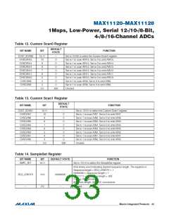
CS
SCLK
DIN
1
16
1
1
ENTRY 1
ENTRY 2
ENTRY N = (SEQ_LENGTH)
DOUT
WRITE SampleSet REGISTER
DEFINE SEQ_LENGTH
LOAD SampleSet PATTERN
TIME BETWEEN CS FALLING AND
RISING EDGE DEPENDS IN SEQ_LENGTH
WRITE ADC MODE CONTROL
OR CONTINUE WITH ADDITIONAL
CONFIGURATION SETTINGS
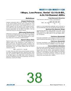
Figure 10. SampleSet Timing Diagram
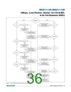
Upon receiving the SampleSet pattern, the user can
set the ADC Mode Control register to begin the conver-
sion process where data readout begins with the first
SampleSet entry. While the last conversion result is read,
the ADC can be instructed to enter AutoShutdown, if
desired. If the user wishes to change the SampleSet
length, a new pattern must be loaded into the ADC as
described in Figure 10.
Layout, Grounding, and Bypassing
For best performance, use PCBs with a solid ground
plane. Ensure that digital and analog signal lines are
separated from each other. Do not run analog and digital
(especially clock) lines parallel to one another or digital
lines underneath the ADC package. Noise in the V
OVDD, and REF affects the ADC’s performance. Bypass
,
DD
the V , OVDD, and REF to ground with 0.1FF and 10FF
DD
bypass capacitors. Minimize capacitor lead and trace
lengths for best supply-noise rejection.
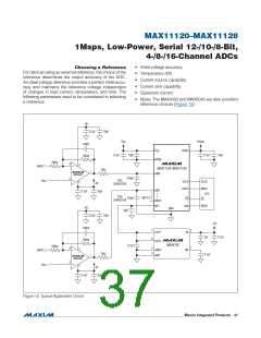
Applications Information
Choosing an Input Amplifier
It is important to match the settling time of the input
amplifier to the acquisition time of the ADC. The conver-
sion results are accurate when the ADC samples the
input signal for an interval longer than the input signal’s
worst-case settling time. By definition, settling time is
the interval between the application of an input voltage
step and the point at which the output signal reaches
and stays within a given error band centered on the
resulting steady-state amplifier output level. The ADC
input sampling capacitor charges during the sampling
cycle, referred to as the acquisition period. During this
acquisition period, the settling time is affected by the
input resistance and the input sampling capacitance.
This error can be estimated by looking at the settling
of an RC time constant using the input capacitance
and the source impedance over the acquisition time
period. Figure 13 shows a typical application circuit. The
MAX4430, offering a settling time of 37ns at 16-bit reso-
lution, is an excellent choice for this application. See the
THD vs. Input Resistance graph in the Typical Operating
Characteristics.
How to Program Modes
1) Configure the ADC (set the MSB on DIN to 1).
2) Program ADC mode control (set the MSB on DIN to 0)
to begin the conversion process or to control power
management features.
•ꢀ IfꢀADCꢀmodeꢀcontrolꢀisꢀwrittenꢀduringꢀaꢀconversionꢀ
sequence, the ADC finishes the present conver-
sion and at the next falling edge of CS initiates its
new instruction.
•ꢀ Ifꢀconfigurationꢀdataꢀ(MSBꢀonꢀDINꢀisꢀaꢀ1)ꢀisꢀwrittenꢀ
during a conversion sequence, the ADC finishes
the present conversion in the existing scan mode.
However, data on DOUT is not valid in following
frames until a new ADC mode control instruction
is coded.
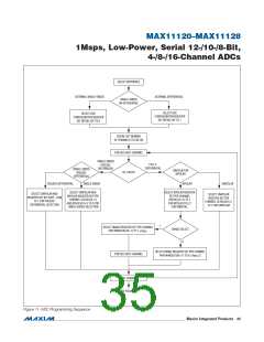
Programming Sequence Flow Chart
See Figure 11 for programming sequence.
���������������������������������������������������������������� Maxim Integrated Products 34

 MAXIM [ MAXIM INTEGRATED PRODUCTS ]