DS2781
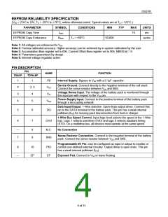
EEPROM RELIABILITY SPECIFICATION
(VDD = 2.5V to 10V, TA = -20°C to +70°C, unless otherwise noted. Typical values are at TA = +25°C.)
PARAMETER
EEPROM Copy Time
SYMBOL
tEEC
CONDITIONS
MIN
TYP
MAX
UNITS
ms
15
EEPROM Copy Endurance
NEEC
TA = +50°C
50,000
cycles
Note 1: All voltages are referenced to VSS.
Note 2: Factory calibrated accuracy. Higher accuracy can be achieved by in-system calibration by the user.
Note 3: Accumulation Bias register set to 00h. Current Offset Bias register set to 00h. NBEN bit = 0.
Note 4: Parameters guaranteed by design.
Note 5: Internal voltage regulator active.
PIN DESCRIPTION
PIN
NAME
FUNCTION
TSSOP
TDFN-EP
1
1
VB
VSS
VIN
Internal Supply. Bypass to VSS with a 0.1µF capacitor.
Device Ground. Connect directly to the negative terminal of the cell stack.
Connect the sense resistor between VSS and SNS.
Voltage Sense Input. The voltage of the battery pack is monitored through
this input pin with respect to the VSS pin.
2
3
4
2, 3
4
Power-Supply Input. Connect to the positive terminal of the battery pack
through a decoupling network.
5
VDD
Data Input/Output. 1-Wire data line. Open-drain output driver. Connect this
pin to the DATA terminal of the battery pack. This pin has a weak internal
pulldown (IPD) for sensing pack disconnection from host or charger.
5
6
6
7
DQ
1-Wire Bus Speed Control. Input logic level selects the speed of the 1-Wire
bus. Logic 1 selects overdrive (OVD) and logic 0 selects standard timing
(STD). On a multidrop bus, all devices must operate at the same speed.
OVD
—
7
8
9
N.C.
SNS
No Connection
Sense Resistor Connection. Connect to the negative terminal of the battery
pack. Connect the sense resistor between VSS and SNS.
Programmable I/O Pin. Can be configured as input or output to monitor or
control user-defined external circuitry. Output driver is open drain. This pin
has a weak internal pulldown (IPD).
8
10
PIO
EP
—
EP
Exposed Pad. Connect to VSS or leave floating.
4 of 31

 MAXIM [ MAXIM INTEGRATED PRODUCTS ]