88E1111 Product Brief
Integrated 10/100/1000 Ultra Gigabit Ethernet Transceiver
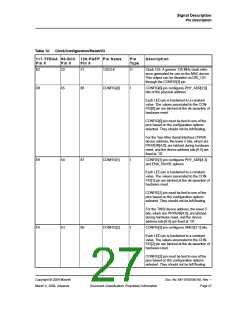
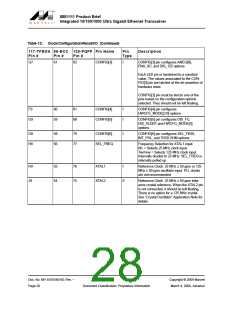
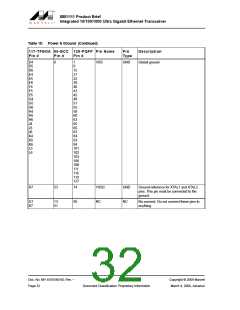
Table 12: Clock/Configuration/Reset/I/O (Continued)
117-TFBGA 96-BCC 128-PQFP Pin Name
Pin
Description
Pin #
Pin #
Pin #
Type
G7
61
82
CONFIG[3]
I
CONFIG[3] pin configures ANEG[0],
ENA_XC, and DIS_125 options.
Each LED pin is hardwired to a constant
value. The values associated to the CON-
FIG[3] pin are latched at the de-assertion of
hardware reset.
CONFIG[3] pin must be tied to one of the
pins based on the configuration options
selected. They should not be left floating.
F9
60
59
81
80
CONFIG[4]
CONFIG[5]
I
I
CONFIG[4] pin configures
HWCFG_MODE[2:0] options.
G9
CONFIG[5] pin configures DIS_FC,
DIS_SLEEP, and HWCFG_MODE[3]
options.
G8
H8
58
56
79
77
CONFIG[6]
SEL_FREQ
I
CONFIG[6] pin configures SEL_TWSI,
INT_POL, and 75/50 OHM options.
Frequency Selection for XTAL1 input
NC = Selects 25 MHz clock input.
Tied low = Selects 125 MHz clock input.
Internally divided to 25 MHz. SEL_FREQ is
internally pulled up.
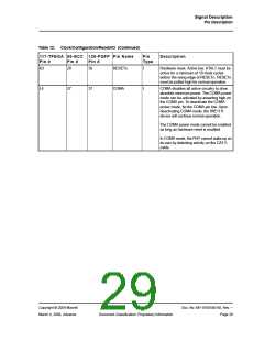
H9
J9
55
54
76
75
XTAL1
XTAL2
I
Reference Clock. 25 MHz ± 50 ppm or 125
MHz ± 50 ppm oscillator input. PLL clocks
are not recommended.
0
Reference Clock. 25 MHz ± 50 ppm toler-
ance crystal reference. When the XTAL2 pin
is not connected, it should be left floating.
There is no option for a 125 MHz crystal.
See “Crystal Oscillator” Application Note for
details.
Doc. No. MV-S105540-00, Rev. --
Page 28
Copyright © 2009 Marvell
Document Classification: Proprietary Information
March 4, 2009, Advance

 MARVELL [ MARVELL TECHNOLOGY GROUP LTD. ]