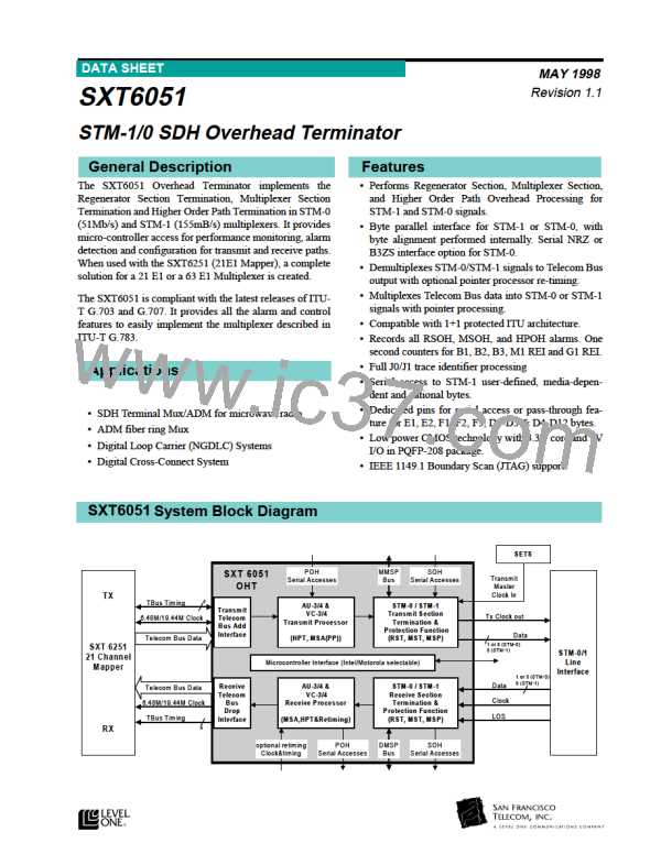
SXT6051 STM-1/0 SDH Overhead Terminator
Table 1: Signal Description Nomenclature
Type
Description
I
Standard input signal
Standard output signal
Input and output signal
Supports TTL input levels
O
I/O
TTLin1
HiZ1
High Impedance
1. Out and I/O signals indicate buffer strength. For example, HiZ-4ma indicates a
high-impedance buffer capable of sourcing 4 ma.
Table 2: Signal Description (Sheet 1 of 11)
Pin #
Name
Type
Description
STM-0 Transmit/ Receive Serial Format
159
160
161
206
205
204
DHPOSD
I
Positive B3ZS or NRZ Data Receive. Input for STM-0 data at
51.84 Mbit/s supplied by the STM-0 line interface unit.
TTLin
DHNEGD
DHICLK
MHPOSD
MHNEGD
MICLK
I
Negative B3ZS Data Receive. Input for STM-0 data at 51.84
Mbit/s when B3ZS coding is used.
TTLin
I
Serial Data Clock Input. Receive STM-0 clock at 51.84 MHz
provided by the external STM-0 line interface unit.
TTLin
O
Positive B3ZS or NRZ Data Transmit. Output of STM-0 data
at 51.84 Mbit/s; either NRZ or B3ZS
HiZ-8ma
O
Negative B3ZS Data Transmit. Output of STM-0 data at
51.84 Mbit/s when B3ZS coding is used.
HiZ-8ma
O
Serial Data Clock Output. The serial output clock of the mul-
tiplexer. This signal is to be used with the serial data MHPOSD
and MHNEGD when needed.
HiZ-8ma
STM1/STM-0 Transmit Receive Parallel Format
172, 171, DHBDATA<7:0>
170, 169,
I
Parallel NRZ Data Receive. Parallel input data in STM-1 or
STM-0 mode.
TTLin
168, 167,
166, 165
173
DHBCLK
I
Parallel Data Clock Input. Parallel input data clock at either
TTLin
19.44 MHz for STM-1 or 6.48 MHz for STM-0
203, 202, MHBDATA<7:0>
201, 200,
O
Parallel NRZ Data Transmit. Parallel output data in STM-1
or STM-0 mode.
HiZ-4ma
198, 197,
196, 195
194
MHBCLKO
O
Parallel Data Clock Output. Parallel output data clock at
HiZ-8ma
either 19.44 MHz for STM-1 or 6.48 MHz for STM-0.
8

 LevelOne [ LEVEL ONE ]