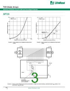
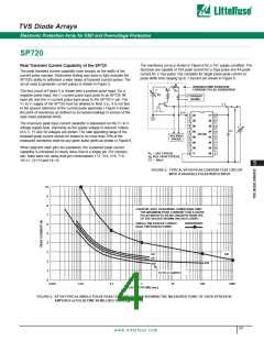
TVS Diode Arrays
Electronic Protection Array for ESD and Overvoltage Protection
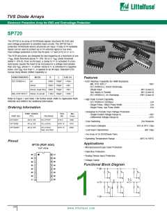
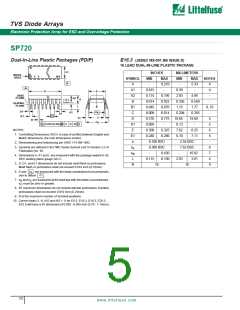
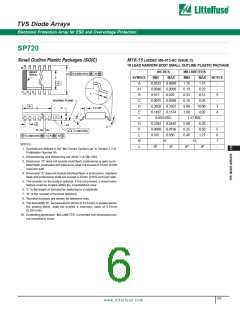
SP720
Small Outline Plastic Packages (SOIC)
M16.15 (JEDEC MS-012-AC ISSUE C)
16 LEAD NARROW BODY SMALL OUTLINE PLASTIC PACKAGE
INCHES MILLIMETERS
N
INDEX
AREA
0.25(0.010)
M
B M
H
E
SYMBOL
MIN
MAX
0.0688
0.0098
0.020
MIN
1.35
0.10
0.33
0.19
9.80
3.80
MAX
1.75
0.25
0.51
0.25
10.00
4.00
NOTES
-B-
A
A1
B
C
D
E
e
0.0532
0.0040
0.013
-
-
1
2
3
L
9
-
SEATING PLANE
A
0.0075
0.3859
0.1497
0.0098
0.3937
0.1574
-A-
3
4
-
o
h x 45
D
-C-
0.050 BSC
1.27 BSC
µ
H
h
0.2284
0.0099
0.016
0.2440
0.0196
0.050
5.80
0.25
0.40
6.20
0.50
1.27
-
e
A1
C
5
6
7
-
B
0.10(0.004)
L
0.25(0.010) M
C
A M B S
N
µ
16
16
NOTES:
o
o
o
o
0
8
0
8
1. Symbols are defined in the “MO Series Symbol List” in Section 2.2 of
Publication Number 95.
5
2. Dimensioning and tolerancing per ANSI Y14.5M-1982.
3. Dimension “D” does not include mold flash, protrusions or gate burrs.
Mold flash, protrusion and gate burrs shall not exceed 0.15mm (0.006
inch) per side.
4. Dimension “E” does not include interlead flash or protrusions. Interlead
flash and protrusions shall not exceed 0.25mm (0.010 inch) per side.
5. The chamfer on the body is optional. If it is not present, a visual index
feature must be located within the crosshatched area.
6. “L” is the length of terminal for soldering to a substrate.
7. “N” is the number of terminal positions.
8. Terminal numbers are shown for reference only.
9. The lead width “B”, as measured 0.36mm (0.014 inch) or greater above
the seating plane, shall not exceed a maximum value of 0.61mm
(0.024 inch).
10. Controlling dimension: MILLIMETER. Converted inch dimensions are
not necessarily exact.
233
www. lit t elf us e. c om

 LITTELFUSE [ LITTELFUSE ]