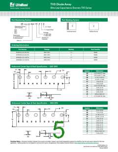
TVS Diode Array
Ultra Low Capacitance Discrete TVS Series
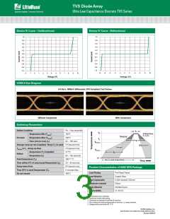
Device IV Curve - Unidirectional
Device IV Curve - Bidirectional
1.0
0.8
1.0
0.8
0.6
0.6
0.4
0.4
0.2
0.2
0.0
0.0
-0.2
-0.4
-0.6
-0.8
-1.0
-0.2
-0.4
-0.6
-0.8
-1.0
-10
-8
-6
-4
0
2
4
6
8
10
-2
-2
-1
0
1
3
4
5
6
7
8
9
10
2
Voltage (V)
Voltage (V)
USB3.0 Eye Diagram
5.0 Gb/s, 1000mV differential, CPO Compliant Test Pattern
Without Component
With Component
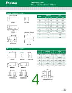
Soldering Parameters
Reflow Condition
-Temperature Min (Ts(min)
-Temperature Max (Ts(max)
-Time (min to max) (ts)
Pb – Free assembly
tP
TP
Critical Zone
to T
)
150°C
TL
P
Ramp-up
Pre Heat
)
200°C
TL
TS(max)
tL
60 – 180 secs
Average ramp up rate (Liquidus) Temp (TL) to peak 3°C/second max
Ramp-down
Preheat
TS(max) toTL - Ramp-up Rate
-Temperature (TL) (Liquidus)
-Temperature (tL)
3°C/second max
217°C
TS(min)
tS
Reflow
60 – 150 seconds
260+0/-5 °C
25
PeakTemperature (TP)
time to peak temperature
Time
Time within 5°C of actual peakTemperature (tp)
Ramp-down Rate
20 – 40 seconds
6°C/second max
8 minutes Max.
260°C
Product Characteristics of 0402 DFN Package
Time 25°C to peakTemperature (TP)
Do not exceed
Lead Plating
Pre-Plated Frame
Copper Alloy
Lead Material
Lead Coplanarity
Substrate material
Body Material
Flammability
0.004 inches(0.102mm)
Silicon
Molded Epoxy
UL 94 V-0
Notes :
1. All dimensions are in millimeters
2. Dimensions include solder plating.
3. Dimensions are exclusive of mold flash & metal burr.
4. Blo is facing up for mold and facing down for trim/form, i.e. reverse trim/form.
5. Package surface matte finish VDI 11-13.
© 2019 Littelfuse, Inc.
Specifications are subject to change without notice.
Revised: 08/22/19

 LITTELFUSE [ LITTELFUSE ]